CDR-830
36
A
B
C
D
1
2
3
4
1
2
3
4
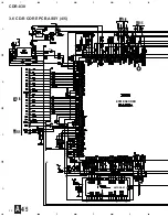
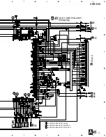
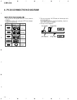
4. PCB CONNECTION DIAGRAM
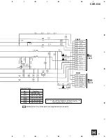
NOTE FOR PCB DIAGRAMS :
1. Part numbers in PCB diagrams match those in the schematic
diagrams.
2. A comparison between the main parts of PCB and schematic
diagrams is shown below.
3. The parts mounted on this PCB include all necessary parts for
several destinations.
For further information for respective destinations, be sure to
check with the schematic diagram.
4. View point of PCB diagrams.
Symbol In PCB
Diagrams
Symbol In Schematic
Diagrams
Part Name
B C E
D
D
G
G
S
S
B C E
B
C
E
D
G
S
B
C
E B
C
E
B
C
E
Transistor
Transistor
with resistor
Field effect
transistor
Resistor array
3-terminal
regulator
Capacitor
Connector
P.C.Board
Chip Part
SIDE A
SIDE B
Summary of Contents for BurnIT CDR-830
Page 45: ...CDR 830 45 A B C D 5 6 7 8 5 6 7 8 G IC701 IC702 IC706 CN601 D SIDE A SIDE B...
Page 71: ...71 CDR 830 Pin Function 2 5...
Page 72: ...72 CDR 830 Pin Function 3 5...
Page 73: ...73 CDR 830 Pin Function 4 5...
Page 74: ...74 CDR 830 Pin Function 5 5...
Page 78: ...78 CDR 830 AK8567 CD R CORE PCB ASSY IC101 RF Processor Pin Function 1 2...
Page 79: ...79 CDR 830 Pin Function 2 2...
Page 82: ...82 CDR 830 1 FL TUBE Grid Assignment Pin Connection PEL1101 OPERATING ASSY V701 7 2 2 DISPLAY...
Page 83: ...83 CDR 830 Anode Connection...
Page 89: ...CDR 830 89 ORDER NO RRV2408M T ZZR DEC 2000 Printed in Japan...

