Package and Layout Guidelines
GS2011M Low Power WiFi Module Data Sheet
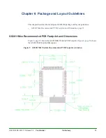
GS2011Mxx Recommended PCB Footprint and Dimensions
54
Confidential
Preliminary
GS2011M-DS-001211, Release 0.9
Figure 9 GS2011MIx Module Dimensions (in inches)
Notes:
1. All Dimensions are in inches. Tolerances shall be + 0.010 inches.
2. Absolutely no metal trace or ground layer underneath this area. If using PCB
antenna, it is recommended to have only air under this area. Hang antenna over
edge of base board or cut notch in base board.
3. It is recommended not to run circuit traces underneath the module especially
near these holes. The RF shield mounting holes are grounded. If traces must be
routed under the GS2011Mxx, it is recommended that extra thick solder mask (5
mils) be used to prevent shorting. High speed signals should be kept as far as
possible from the antenna and RF areas of the GS2011Mxx.
4. In performing SMT or manual soldering of the module to the base board, first
align the row of pins from #18 through #31 onto the base board and then match
the other two rows.
In additional to the guidelines, note the following suggestions:
1. External Bypass capacitors for all module supplies should be as close as
possible to the module pins.
2. Never place the antenna very close to metallic objects.
3. External monopole antennas need a reasonable ground plane area for antenna
efficiency.
4. Do not use a metallic or metalized plastic for the end product enclosure when
using on-board antenna.
5. If the module is enclosed in a plastic case, have reasonable clearance from
plastic case to on-board antenna.

