GS2011M Architecture
GS2011M Low Power WiFi Module Data Sheet
Wireless LAN and System Control Subsystem
32
Confidential
Preliminary
GS2011M-DS-001211, Release 0.9
The following are not system states, but are related design notes:
Power Control:
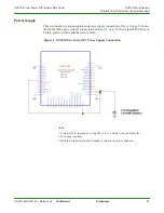
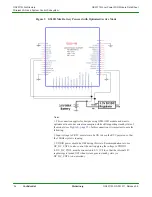
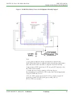
The GS2011M was designed with the intent that power to the
non-RTC portions of the chip be controlled from the DC_DC_CNTL signal. In
applications where it is preferred that an external host control the power, this is OK if
ALL power, including VRTC power, is turned on and off by the external host. In this
case, all state is lost when power goes off, and the latencies from first battery plug
apply.
If these latencies are not acceptable, then the GS2011M MUST control power. The
external host would use an alarm to wake it up, and a serial command to put it into
standby. The DC_DC_CNTL pin would control the power supplies. It is NOT reliable
for the external host to directly control the power supplies if VRTC is to be left turned
on. This is because the RTC would not know when to isolate itself from the rest of the
chip, and might get corrupted during power up or power down.
EXT_RESET_n pin:
If the external host is driving the EXT_RESET_n pin, it MUST
do so with an open drain driver. This is because this pin is driven low during power up
by the RTC. In addition, if an external host is connected to the EXT_RESET_n pin,
there must be an external 10K ohm pull-up resistor on the board, pulling up to VDDIO.
This is needed to overcome a possible pull-down in the host at first power application.
It is also recommended that the host not actively assert EXT_RESET_n until all the
startup latencies have expired.
NOTE:
For the above power states, software controls which clocks stay turned
on in each of the three states.

