GS2011M Low Power WiFi Module Data Sheet
GS2011M Architecture
Wireless LAN and System Control Subsystem
GS2011M-DS-001211, Release 0.9
Confidential Preliminary
31
In standby state, the 32.768KHz oscillator keeps running and only the RTC RAM
retains the state (how many banks retain their state is SW configurable). SRAM, CPUs
and I/Os are all in OFF state, as there is no 1.8V and no VDDIO being supplied to the
GS2011M device.
This is the lowest-power-consumption state. In a typical application, the system returns
to the Standby state between periods of activity, to keep the average power very low
and enable years of operation using conventional batteries. During standby, the RTC
isolates itself from the rest of the chip, since the signals from the rest of the chip are
invalid. This prevents corruption of the RTC registers.
Exit from standby occurs when a pre-specified wakeup time occurs, or when one of the
RTC_IO’s configured as alarm inputs sees the programmed polarity of signal edge.
When one of the wakeup conditions occurs, the RTC asserts reset to the chip and sets
the DC_DC_CNTL pin high to enable power to the rest of the module. After power to
the rest of the module is assumed to be good, the isolation between the RTC and the
rest of the chip is released, and the EXT_RESETn pin is released. The system now
starts booting.
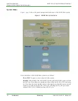
System Configuration
: When a power-up is requested, the system transitions from the
Standby state to the System Configuration state. In this state, the APP CPU is released
from reset by the RTC. The WLAN CPU remains in the reset state during System
Configuration. The APP CPU then executes the required system configurations,
releases the WLAN CPU from reset, and transitions to the Power-ON state.
The System Configuration state is also entered on transition from the Power-ON state
to the Standby state, to complete necessary preparations before shutting off the power
to the core system.
Power-ON
: This is the active state where all system components can be running. The
Power-ON state has various sub-states, in which unused parts of the system can be in
sleep mode, reducing power consumption. Sleep states are implemented by gating the
clock signal off for a specific system component. Additionally, unneeded clock sources
can be turned off. For example, receiving data over a slave SPI interface could be done
with only the 80MHz RC oscillator active, and the 40MHz crystal and PLL turned off.
Sleep:
In the Sleep state, the 40MHz crystal and the 80MHz RC oscillator remains
running, but it is gated off to one or both CPUs. Each CPU can independently control
its own entry into Sleep state. Any enabled interrupt will cause the interrupted CPU to
exit from Sleep state, and this will occur within a few clock cycles.
Deep Sleep:
Deep sleep is entered only when both CPUs agree that the wakeup latency
is OK. In Deep Sleep mode, the 40MHz crystal oscillator and 80MHz RC oscillator are
turned off to save power, but all power supplies remain turned on. Thus all registers,
memory, and I/O pins retain their state. Any enabled interrupt will cause an exit from
Deep Sleep state.
NOTE:
During first battery plug, i.e., when power is applied the first time to the
RTC power rail (VRTC), the power detection circuit in the RTC also causes a
wakeup request.

