background image

1-13-26

P

b

F

1

1

BE3TK3F01028

1

BE3TK3F0102 8D

1

YELLOW

WHITE

RED

J2002

CN2001

C2010

C2012

D2003

D2007

D2008

D2009

R2005

R2006

R2007

R2008

D2010

Q2003

Q2002

JK3001

JK3002

JK3003

J3001

J3601

D3014

CN3605

1

4

F

1

4

1

4

15

1

1

1

1

V-14

15

BE3TK3F0102

         8C

V-14

HDD-DVD

OPEN/CLOSE

VCR-DVD

V-14

BE3TK3F0102

         8B

RESET

HDD/REC

DVD/REC

DVD

T

W

T

L2003

C2001

C2002

C2009

D2001

D2002

D2004

R2001

D2005

D2006

R2003

D2011

D2012

JK2001

Q2001

C1156

CN6005

IC1190

CN3003

SW3008

SW30

10

D3012

SW3681

SW3682

W

D3013

J3002

CN3011

CN3012

SW3001

D3001

D3002

D3003

R3001

R3003

R3022

J3603

CN3604

SW3404

SW3005

SW3402

SW3002

D3403

SW3004

SW3403

HDD

VCR

D3004

D3005

R3004

R3010

R3011

SW3006

D340

5

1

1

DIP

OPEN/CLOSE

DUBBING

SW3009

T

BE3TK3F0102

CN6001

V-14

USB PCB

1

4

1

SW3007

CN6002

8E

4

1

4

D1602

D1605

D1601

SW1601

SW671

D671

CN1602

BE3TK3F0102

8 G

SW675

V-14

1

RL1001

JP954

COLD

HOT

K

K

K

K

K

K

D1151

Q1051

C1057

D1055

D1057

R1053

D1058

R1054

R1055

R1058

IC1051

C1053

D1050

D1059

D1056

L1006

D1052

L1007

D1053

D1054

K

Q1119

D1122

C1151

D1152

D1153

D1157

R1157

1

C1056

J1041

J1042

D1145

T1051

D1161

GND

J1044

J1039

G

ND

C1128

IC1103

D1112

C1146

CN1001

30

VIN+1.2V

SPDIF

+1.8V

MAIN-ON

D1136

J1038

J1040

J1043

F

Ver.14

Q1114

C1119

Q1115

IC1102

C1132

D1116

D1117

R1118

C1140

D1131

D1132

R1134

R1163

R1164

R1170

R1175

R1177

R1190

CN1003

C1039

L1101

Q1100

Q1101

Q1102

Q1104

Q1112

+12V

D1135

J1019

J1033

D1109

+5V

J1021

+44V

J1018

JP1014

+44V

J1020

B

E

C

C1129

IC1104

D1120

D1123

C013

C1152

D1140

R1141

D1154

D1159

D1162

D017

D019

C1037

P-ON+3V3

Q1107

Q1109

GND

J1023

+12V

REG-CONT

LATCH-UP

GND

GND

D1034

D1033

J1028

J1029

J1027

J1030

J1035

J1032

J1036

J1037

J1031

D1150

R1183

J1022

L11

51

J1050

K

7.5mm

pitch

IC1151

R1161

C1006

C1052

C1102

C1007

IC1052

C1002

C1050

C1051

D013

C015

C016

K

K

K

K

BE3TK3F0102 

8-A

V-14

L1003

D1004

R1003

R1005

D1003

D1001

C1005

D1051

C1004

D1002

T2.5A H 250V

BROWN

BLUE

L1001

L1002

AC1001

C1001

R1001

D1006

F1001

SA1001

R1009

D1009

R1004

D1023

R1036

J1045

Q1003

R1006

R1007

R1008

R1029

R1

C1133

Q1001

C10

29

C1030

IC1001

C1031

C1034

D1011

D1022

D1025

R1031

R1033

R1037

R1039

R1043

L1004

C1003

D1005

L1008

L1005

D1101

D1102

IC1101

R1110

R1111

C020

D014

C1035

C1036

C1100

C1105

C1107

J1012

J1013

C1110

T1001

GND

J1011

J1009

C014

D016

D1032

D1103

D018

D020

C1121

C1127

R1104

D1108

R1126

L1013

C022

R1137

R1140

D1163

CN1002

C1038

GND

+5V

J1002

F1

J1003

F2

J1004

+5V

J1005

+16V

J1006

+12V

J1007

C1104

Q1105

Q1106

+1.8V

J1017

C1114

C1115

J1010

J1008

J1015

+5V

D1146

34

C1108

J1016

P

-ON+3V3

L1014

1V2CONT

J1001

CL1001

1

BE3TK3F01028

NOTE:

The voltage for parts in hot circuit is measured using
hot GND as a common terminal.

CAUTION !

For continued protection against fire hazard,
replace only with the same type fuse.

CAUTION !

Fixed voltage (or Auto voltage selectable) power supply circuit is used in this unit.
If Main Fuse (F1001) is blown , check to see that all components in the power supply
circuit are not defective before you connect the AC plug to the AC power supply.
Otherwise it may cause some components in the power supply circuit to fail.  

Because a hot chassis ground is present in the power supply 
circuit, an isolation transformer must be used when repairing.
Also, in order to have the ability to increase the input slowly, 
when troubleshooting this type of power supply circuit, 
a variable isolation transformer is required. 

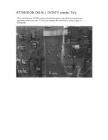
Power Supply, Function, SW, Rear Jack, USB & Power SW CBA Top View

SW CBA

Function CBA

Rear Jack CBA

USB CBA

Power SW CBA

Power Supply CBA

Summary of Contents for WD6D-M100

Page 1: ...M100 Main Section I Specifications I Preparation for Servicing I Adjustment Procedures I Schematic Diagrams I CBA I Exploded Views I Parts List When servicing the deck mechanism refer to MK14 Deck Me...

Page 2: ...Initialize the DVD recorder VCR 1 8 1 Firmware Renewal Mode 1 9 1 Function Indicator Symbols 1 10 1 Troubleshooting 1 11 1 Block Diagrams 1 12 1 Schematic Diagrams CBA and Test Points 1 13 1 Waveform...

Page 3: ...o recording format Sampling frequency Compression format 48 kHz Dolby Digital Tuner Analogue channels L SECAM L BG PAL B G F1 E69 E2 E69 DVB T channels VHF UHF F5 F10 E21 E69 Available source coding m...

Page 4: ...way from the pickup lens when the diode is turned on Do not look directly at the laser beam CAUTION Use of controls and adjustments or doing procedures other than those specified herein may result in...

Page 5: ...rious radiation These must also be replaced only with specified replacements Examples RF converters RF cables noise blocking capacitors and noise blocking filters etc C Use specified internal wiring N...

Page 6: ...parts RF terminals antenna terminals video and audio input and output terminals microphone jacks earphone jacks etc is lower than or equal to the specified value in the table below Measuring Method P...

Page 7: ...achine then apply hot air to the Flat Pack IC about 5 to 6 seconds Fig S 1 1 2 Remove the flat pack IC with tweezers while applying the hot air 3 Bottom of the flat pack IC is fixed with glue to the C...

Page 8: ...by one using a sharp pin or wire to which solder will not adhere iron wire When heating the pins use a fine tip soldering iron or a hot air desoldering machine Fig S 1 4 3 Bottom of the flat pack IC i...

Page 9: ...s Fig S 1 6 Note When using a soldering iron care must be taken to ensure that the flat pack IC is not being held by glue When the flat pack IC is removed from the CBA handle it gently because it may...

Page 10: ...ed to remove any static electricity that may be charged on the body 2 Ground for Workbench Be sure to place a conductive sheet or copper plate with proper grounding 1 M on the workbench or other surfa...

Page 11: ...into the Deck Mechanism Assembly and press B VCR button The tape will be loaded into the Deck Mechanism Assembly Make sure the power is on connect JP278 S INH to GND This will stop the function of Ta...

Page 12: ...mbly D3 S 6 2 S 7 2 S 8 2 S 9 CN101 CN502 CN701 CN901 CN981 Dust Cover Mecha Earth Plate Hook 2 6 Fan Holder D4 2 S 10 CN1002 1 Top Cover 2 Front Assembly 4 Front Bracket 20 Front Bracket R 21 Bracket...

Page 13: ...Before installing the Deck Assembly be sure to place the pin of LD SW on the AV CBA as shown in Fig D7 Then install the Deck Assembly while aligning the hole of Cam Gear with the pin of LD SW the sha...

Page 14: ...r Panel 1 1 See Reference Note 5 Earth Spring Fig D4 FFC Guide Mode Lens Holder CL1001 CN3605 S 17 S 18 S 14 S 15 S 16 9 Power Supply CBA 10 Power Holder 12 Function CBA 11 SW CBA Desolder CN1504 Fig...

Page 15: ...ear Jack CBA FE Head Cylinder Assembly ACE Head Assembly 18 AV CBA SW507 LD SW From FE Head BOTTOM VIEW Lead connections of Deck Assembly and AV CBA Desolder FFC of Capstan Motor Printing side Desolde...

Page 16: ...1 6 5 E9TFCDC S 24 S 25 S 26 DV Earth Plate DV Cable S 27 19 Deck Pedestal 21 Bracket R 20 Front Bracket R Fig D8...

Page 17: ...e the Top Cover Front Assembly Front Bracket DVD Mechanism DVD Main CBA Assembly 2 Remove the Dust Cover 3 Rotate the gear in the direction of the arrow manually as shown below the tray descends 4 Pul...

Page 18: ...e 0 001 50V Div F Range DC AC 20MHz 2 Alignment Tape FL6A Head Switching Position Adjustment Purpose To determine the Head Switching position during playback Symptom of Misadjustment May cause Head Sw...

Page 19: ...eted the DVD recorder VCR exits the Version display mode and turns off the power automatically To move into the Normal mode from the Version display mode press RETURN BACK button on the remote control...

Page 20: ...en Firmware Updating XX Complete is displayed on the screen BE version number is displayed on the VFD such as 194000 Fig d Programming Mode Screen Fig e VFD in Version Up Mode Example The appearance s...

Page 21: ...the firmware version Display Contents MODEL NAME Model Name DVB T VERSION DVB T Module version FE VERSION Firmware F E version BE VERSION Firmware B E version TT VERSION Firmware T T version DV UNIQUE...

Page 22: ...n reel or capstan mechanism is not functioning correctly A R is displayed on a TV screen Refer to Fig 1 When tape loading mechanism is not functioning correctly A T is displayed on a TV screen Refer t...

Page 23: ...te the data after recovering SMALL VMGI 15 Cannot write the data after DVD R Reverse Track 16 An error occurs in Finalize Close 17 An error occurs in Rec Stop Close 18 An error occurs in PCA Full DVD_...

Page 24: ...ation Area is full Insert a new disc 35 PCA is Full in REC start This disc is already finalized Release the finalizing for this disc 36 It is finalized Video Format Disc Can not record on this disc Re...

Page 25: ...heck the presence that the primary component is leaking or shorted and service it if defective Check the presence that the rectifying diode or circuit is shorted in each rectifying circuit of secondar...

Page 26: ...140 and their periphery and service it if defective Check D1526 R1634 R1635 and their periphery and service it if defective FLOW CHART NO 9 P ON 9V VCR is not outputted Is 12V voltage supplied to coll...

Page 27: ...Refer to FLOW CHART NO 9 P ON 9V VCR is not outputted No Yes Check Q1517 and their periphery and service it if defective FLOW CHART NO 13 ECO 5V is not outputted Is 5V voltage supplied to collector o...

Page 28: ...7 D1031 and their periphery and service it if defective No Yes Check Q1100 Q1101 Q1104 POW SW line and their periphery and service it if defective Check for short circuiting or leak on the load circui...

Page 29: ...supplied to Pin 1 of IC1103 No Yes Yes Check D1033 and their periphery and service it if defective No Check IC3607 IC3608 and their periphery and service it if defective No Is 5V voltage supplied to P...

Page 30: ...switches FLOW CHART NO 2 No DVD operation is possible from the remote control Operation is possible from the unit Replace RS1501 remote control receiver or remote control unit Check the line between...

Page 31: ...11PIN 18PIN Continued to A on the next page Check the ECO 5V ECO 9V line and service it if defective Replace IC1509 Yes No Is 5V voltage supplied to Pin 27 29 47 63 of IC1509 Is 9V voltage supplied to...

Page 32: ...t the disc on the disc tray and playback it Are the video signals outputted to each pin of IC1509 Yes Yes No Are the video signals outputted to each pin of CN1502 Replace DVD MECHANISM DVD MAIN CBA AS...

Page 33: ...each pin of CN1502 and service it if defective Are the audio signals outputted to Pin 79 80 of IC1509 Yes Are the audio signals outputted to Pin 11 13 of CN1502 Yes Yes No No No IC1509 AUDIO IN1 AV1...

Page 34: ...02 17PIN AUDIO L OUT CN1502 15PIN AUDIO R OUT Check the periphery between Pin 73 74 of IC1509 and the audio terminal JK1504 and service it if defective Are the audio signals outputted to the specific...

Page 35: ...TOP EJECT Terminal voltage of IC501 7 KEY 1 IC501 7 V Replace the RS1501 remote control receiver or the remote control unit Check the line between the RS1501 remote control receiver and Pin 14 of IC50...

Page 36: ...ecified voltage approximately 13V outputted to the terminal of the Loading Motor Unit When loading a cassette tape does the LD SW operate normally When loading a cassette tape is the specified voltage...

Page 37: ...P ON 5V line and service it if defective Check the line between Pin 8 of CN502 and Pin 77 of IC501 and service it if defective Replace IC501 No No No No No No No No No No No Yes Yes Yes Is 5V voltage...

Page 38: ...to Pin 58 of IC501 Is 5V voltage supplied to Pin 18 24 42 55 72 91 of IC301 Is the serial data and clock signal supplied to Pin 68 69 of IC301 Check the P ON 5V line and service it if defective Check...

Page 39: ...als outputted to the audio terminal JK2001 Yes IC1509 73 74PIN AUDIO OUT 1 AV1 IC1509 71 72PIN AUDIO OUT 2 AV2 Are the audio signals outputted to each pin of IC1509 No No Check the line between Pin 71...

Page 40: ...05 Q406 and service it if defective Replace IC451 Replace the Cylinder Assembly No Replace IC301 No FLOW CHART NO 12 Hi Fi audio can not be recorded normally E E mode is normal Is the Hi Fi COM signal...

Page 41: ...DRV CLK 70 DRV STB DRV DIN DRV CLK DRV STB 69 7 23 25 42 36 8 9 IIC BUS SCL D V SYNC D REC H RF SW H A SW C ROTA IIC BUS SDA H A COMP V ENV C SYNC C SYNC IIC BUS SCL LD SW 9 AL 5V SW507 LD SW AL 5V D...

Page 42: ...EY SWITCH CN1504 CN3011 CN3012 CN3003 CN1505 POWER LED 1 3 POWER SW 2 2 3 2 FUNCTION CBA SW CBA CN3011 CN1504 FUNCTION CBA 7 8 25 29 30 63 66 65 39 38 36 35 SYS RESET SUB RXD SUB TXD 67 64 SUB SCLK RD...

Page 43: ...0 7 N23 U25 SPDIF PCM BCK PCM LRCK PCM SCLK PCM DATA0 P1 D3 D1 N2 M1 N3 M2 VIDEO CLOCK VIDEO CLOCK C5 IC104 IC105 FLASH MEMORY LINK I F LINK I F RECEIVE DATA DECODER TRANSMIT DATA ENCODER FLASH MEMOR...

Page 44: ...01 VIDEO IN2 10 10 VIDEO IN2 20 JK2001 VIDEO IN1 20 JK1504 11 VIDEO G IN 13 13 7 VIDEO B IN 12 12 15 VIDEO OUT1 VIDEO G VIDEO B VIDEO R 19 11 7 15 VIDEO R IN 14 14 JK1504 12 62 18 14 20 SW SW SW SW II...

Page 45: ...79 78 AGC VXO OSD CHARACTER MIX FBC 1 2 58 59 65 29 28 69 68 46 43 84 83 71 62 70 D REC H 80 TP301 C PB WF3 AV CBA TP504 RF SW WF2 X301 4 43MHz C SYNC C SYNC 67 PB VIDEO SIGNAL BUFFER Q402 WF1 48 56...

Page 46: ...01 AUDIO R IN2 AUDIO L OUT2 AUDIO R OUT2 2 AUDIO L IN2 6 1 3 JK1504 AUDIO R IN1 AUDIO L OUT1 AUDIO R OUT1 2 AUDIO L IN1 6 1 3 79 80 70 69 76 77 90 67 68 87 85 92 82 94 89 86 84 91 81 93 SW SW SW SW 72...

Page 47: ...DIO HD SW CONTROL MUTE 11 6 PB ON SP LP ON P R ALC DET ALC IC301 AUDIO SIGNAL PROCESS 13 4 AUDIO PB REC CN504 3 A COM 1 AE H 2 FE H AUDIO HEAD AUDIO ERASE HEAD ACE HEAD ASSEMBLY FE HEAD 2 FE H 1 FE H...

Page 48: ...8 39 75 73 26 21 24 27 N A REC VCR AUDIO OUT R VCR AUDIO OUT L LIM 80 N A PB Hi Fi H SW A MODE TO AUDIO BLOCK DIAGRAM TO AUDIO SELECTOR BLOCK DIAGRAM IIC BUS SDA VCR AUDIO IN L VCR AUDIO IN R IIC BUS...

Page 49: ...3V 30 31 AL 2 8V 27 REG CONT 29 POW SW 34 LATCH UP 10 1V2CONT 23 F2 24 F1 26 SYS 5V 15 16 AL 5V 13 14 DVD P ON 5V 12 P ON 10V 6 7 AL 12V 2 3 AL 16 3V 1 AL 44V 22 AL 30V IC1051 3 4 IC1052 ERROR VOLTAGE...

Page 50: ...16 C POW SW P ON 9V VCR P ON 12V DVD P ON 5V AL 5V AL 12V 2 ECO 12V P ON 5V DECK P ON 5V VCR SYS 5V F1 F2 ECO 9V P ON 1 8V P ON 3 3V ECO 5V 1V2CONT POW SW REG CONT ECO MODE Q1521 9V REG Q1520 Q1528 1...

Page 51: ...ATA0 SPI DATA1 SPI CLK SPI CE 44 VIDEO ENCODER AUDIO INTERFACE AUDIO D A CONVERTER 6 6 TU SDA 5 5 TU SCL 15 15 DTV TXD DTV TXD DTV RXD DTV SYS RESET 14 14 DTV RXD 12 12 DTV SYS RESET 9 10 CN1800 L CH...

Page 52: ...in the schematic diagram and the parts list Before replacing any of these components read the parts list in this manual carefully The use of substitute replacement parts that do not have the same saf...

Page 53: ...n original function and reliability of repaired units use only original replacement parts which are listed with their part numbers in the parts list section of the service manual 4 Voltage indications...

Page 54: ...1 13 3 E9TFASCAV1 AV 1 10 Schematic Diagram VCR Section...

Page 55: ...d f g c e a b d f g c e a b d f g c e a b d f g c e a b FL601 MATRIX CHART PM BS CS DR CD VCR DB HDD DVD DTV T C NOTE These components IC700 R706 R707 can be used in any models However you cannot mix...

Page 56: ...1 13 5 E9TFASCAV3 AV 3 10 Schematic Diagram VCR Section...

Page 57: ...1 13 6 E9TFASCAV4 AV 4 10 Schematic Diagram VCR Section...

Page 58: ...1 13 7 E9TFASCAV5 AV 5 10 Schematic Diagram VCR Section...

Page 59: ...1 13 8 E9TFASCAV6 AV 6 10 Schematic Diagram VCR Section...

Page 60: ...1 13 9 E9TFASCAV7 AV 7 10 Schematic Diagram VCR Section...

Page 61: ...1 13 10 E9TFASCAV8 AV 8 10 Schematic Diagram VCR Section...

Page 62: ...1 13 11 E9TFASCAV9 AV 9 10 Schematic Diagram VCR Section...

Page 63: ...1 13 12 E9TFASCAV10 AV 10 10 Schematic Diagram VCR Section...

Page 64: ...circuit is measured using hot GND as a common terminal CAUTION Fixed voltage or Auto voltage selectable power supply circuit is used in this unit If Main Fuse F1001 is blown check to see that all com...

Page 65: ...4 E9TFASCF Function SW USB Schematic Diagram VCR Section CAUTION For continued protection against fire hazard replace only with the same type fuse F6001 NOTE Either IC3607 or IC3608 is used for FUNCTI...

Page 66: ...1 13 15 Rear Jack Schematic Diagram VCR Section E9TFASCRJ...

Page 67: ...in 1 7 Schematic Diagram DVD Section The order of pins shown in this diagram is different from that of actual IC101 IC101 is divided into six and shown as IC101 1 6 IC101 6 6 in this DVD Main Schemati...

Page 68: ...in 2 7 Schematic Diagram DVD Section The order of pins shown in this diagram is different from that of actual IC101 IC101 is divided into six and shown as IC101 1 6 IC101 6 6 in this DVD Main Schemati...

Page 69: ...in 3 7 Schematic Diagram DVD Section The order of pins shown in this diagram is different from that of actual IC101 IC101 is divided into six and shown as IC101 1 6 IC101 6 6 in this DVD Main Schemati...

Page 70: ...in 4 7 Schematic Diagram DVD Section The order of pins shown in this diagram is different from that of actual IC101 IC101 is divided into six and shown as IC101 1 6 IC101 6 6 in this DVD Main Schemati...

Page 71: ...in 5 7 Schematic Diagram DVD Section The order of pins shown in this diagram is different from that of actual IC101 IC101 is divided into six and shown as IC101 1 6 IC101 6 6 in this DVD Main Schemati...

Page 72: ...1 13 21 E9TFASCD6 DVD Main 6 7 Schematic Diagram DVD Section...

Page 73: ...in 7 7 Schematic Diagram DVD Section The order of pins shown in this diagram is different from that of actual IC101 IC101 is divided into six and shown as IC101 1 6 IC101 6 6 in this DVD Main Schemati...

Page 74: ...1 13 23 E9TFASCDTV DTV Module Schematic Diagram DVD Section...

Page 75: ...UT S CLOCK ECO MODE ECO 5V P ON 9V ECO 12V ZERO 1V2 CONT ALL SYS 5V P DOWN H READY BUSY S DATA IN G3 FL GND DVD REC LED HDD REC LED DVD LED VCR LED F2 GND GND GND ECO 5V ALL SYS 5V VM 15V DM LD ALL 5V...

Page 76: ...X501 X502 C706 VR501 C334 C335 C534 C340 C343 C345 C549 C550 C553 D301 L251 CN1505 TP504 JK1 8P OUT1 D523 DVD SC2 A MUTE C344 Q1547 SW674 SW673 L452 TP301 DVD SC2 A MUTE 1 8V GND ALL 5V DUBBING LED DV...

Page 77: ...J1036 J1037 J1031 D1150 R1183 J1022 L 1 1 5 1 J1050 K 7 5mm pitch IC1151 R1161 C1006 C1052 C1102 C1007 IC1052 C 1 0 0 2 C1050 C1051 D013 C015 C016 K K K K BE3TK3F0102 8 A V 14 L1003 D 1 0 0 4 R1003 R1...

Page 78: ...R1119 R1130 R1131 R1132 R1133 R1135 R1166 R1167 R1171 D1144 A C1129 IC1104 R1111 D1120 C013 D1140 R1141 D1162 D014 D017 D019 C1035 C1037 C1038 P ON 3V3 Q1105 Q1107 GND J1023 12V D1034 D1033 J1028 J102...

Page 79: ...s WF10 Pin 28 of CN1503 WF4 Pin 7 of CN1502 VIDEO Y 0 2V 20 s WF5 Pin 9 of CN1502 VIDEO C 0 2V 20 s WF6 Pin 30 of IC1509 VIDEO CVBS 0 5V 20 s NOTE Input COLOR BAR SIGNAL WITH 1KHz AUDIO SIGNAL WF3 WF...

Page 80: ...1 DTV SYS RESET 2 DTV TXD 3 DTV RXD 4 DTV S SCLK NU 5 BOOTSTRAP NU 6 TO DVD MAIN CBA CN981 W14 CN506 V BUS 1 OC 2 DM 3 DP 4 GND 5 AL 12V 6 AL 12V 7 GND 8 GND 9 AL 5V 15 AL 5V 16 GND 18 LACTH UP 34 POW...

Page 81: ...D ENABLE 15 LDD OSCEN 16 GND 17 LDD WEN4 18 GND 19 LDD WEN3 20 GND 21 LDD WEN2 22 LDD SEL1 23 PD VC 24 PD VSW 25 F 26 G 27 H 28 E 29 RF 30 RF 31 A 32 B 33 C 34 D 35 PD FSPD VCC 36 GND 37 GND 38 FSPD V...

Page 82: ...or Control Signal 26 IN DVD AUDIO MUTE DVD Audio Mute Control Signal Mute L 27 OUT VCR AUDIO MUTE VCR Audio Mute Control Signal Mute L 28 IN A MODE Hi Fi Tape Defection Signal 29 OUT DVD AUDIO MUTE DV...

Page 83: ...Signal to High 76 OUT C CONT Capstan Motor Control Signal 77 OUT D CONT Drum Motor Control Signal 78 OUT C F R Capstan Motor FWD REV Control Signal FWD L REV H 79 IN S REEL Supply Reel Rotation Signal...

Page 84: ...ace Input 10 NU Not Used 11 NU Not Used 12 VSS Ground 13 VDD Power Supply 14 NU Not Used 15 NU Not Used 16 NU Not Used 17 NU Not Used 18 NU Not Used 19 NU Not Used 20 OUT P1 Segment Output Serial Data...

Page 85: ...ote A Anode K Cathode E Emitter C Collector B Base R Reference G Gate D Drain S Source UTC0832 PQ070XFC1SZF PS2561A 1 V A W 2SK3566 STA4 Q M MIP2F10MS 2SA1980MG AT SRC1203MAT 2SA1266G 2SA1980G 2SC3198...

Page 86: ...G G C C W14 W15 W16 B14 B56 L11 L6 L6 B6 L7 B27 B13 L8 B11 B14 L6 L8 L8 L8 L5 L16 A5 L4 L20 L17 B30 A16 L8 L8 L8 L12 L6 L10 L6 L8 B34 L6 B12 L19 L8 A7 B20 A2 B28 B8 L10 L6 B18 W6 L9 L2 B9 B24 W9 W10 B...

Page 87: ...1 18 2 E9TFAPEX Packing Inside Outside Inside Outside S2 A9 S7 S3 S5 S1 S1 X1 X5 X6 X32 X2A X2B S6 X32 S1 S6 FRONT X2C X23 X26...

Page 88: ...B HOLDER E3TK0FD 1VM329013B B34 USB EARTH PLATE E3TK0FD 1VM329052 B57 EARTH SPRING EAB30AD 1VM443463 1B1 DECK ASSEMBLY CZD014 VM25E0 N25E1FL FM1001 MOTOR DC FAN 2D65BK100230 MMEZR12XNR04 L1 SCREW TAP...

Page 89: ...10pF 50V CHD1JD3CH100 C342 CHIP CERAMIC CAP 1608 B K 1000pF 50V CHD1JK30B102 C343 ELECTROLYTIC CAP 10 F 16V M H7 CED100TSK028 C344 ELECTROLYTIC CAP 4 7 F 25V M NP H7 CP1EMAVSB4R7 C345 ELECTROLYTIC CAP...

Page 90: ...1608 B K 1000pF 50V CHD1JK30B102 C700 CHIP CERAMIC CAP 1608 F Z 0 1 F 50V CHD1JZ30F104 C701 ELECTROLYTIC CAP 4 7 F 25V M H7 CEE4R7TSK028 C702 CHIP CERAMIC CAP B K 0 018 F 50V CHD1JK30B183 Ref No Desc...

Page 91: ...1608 CH J 1000pF 50V CHD1JJ3CH102 C1814 ELECTROLYTIC CAP 100 F 6 3V M CEA101TSK012 C1815 ELECTROLYTIC CAP 100 F 6 3V M CEA101TSK012 C1816 CHIP CERAMIC CAP 1608 F Z 0 1 F 50V CHD1JZ30F104 C1825 CHIP CE...

Page 92: ...rt No L1601 BEAD CORE ASSEMBLY E3TK3FD 1VSA22787 L1802 CHIP INDUCTOR LK16081R8K T 1 8UH LLACKB3TU1R8 L1803 CHIP INDUCTOR LK16081R8K T 1 8UH LLACKB3TU1R8 L1901 CHOKE COIL 22 H K LLBD00PKV021 L1904 CHOK...

Page 93: ...k RCG223PAK001 R523 RES CARBON FILM 1 4W G 1 5 k RCG152PAK001 R525 RES CHIP 1608 1 10W J 330 k RRXA334HH013 R526 RES CARBON FILM 1 4W J 330 k RCJ334PAK001 Ref No Description Part No R528 RES CARBON F...

Page 94: ...608 1 10W J 100 k RRXA104HH013 R1704 RES CHIP 1608 1 10W J 820 RRXA821HH013 R1705 RES CHIP 1608 1 10W J 100 k RRXA104HH013 Ref No Description Part No R1706 RES CHIP 1608 1 10W J 820 RRXA821HH013 R1708...

Page 95: ...WIRE CP STP S 0 60 XZ40F0REN002 JP90 WIRE CP STP S 0 60 XZ40F0REN002 JP187 WIRE CP STP S 0 60 XZ40F0REN002 JP237 WIRE CP STP S 0 60 XZ40F0REN002 JP238 WIRE CP STP S 0 60 XZ40F0REN002 JP240 WIRE CP ST...

Page 96: ...DIODE BA159 NDQZ000BA159 D1057 DIODE ZENER 27BSB T26 NDTB027BST26 D1058 DIODE ZENER 27BSB T26 NDTB027BST26 Ref No Description Part No D1059 RECTIFIER DIODE BA159 NDQZ000BA159 D1061 DIODE SWITCHING SMD...

Page 97: ...CHIP 1608 1 10W J 47 k RRXA473HH013 R1167 RES CHIP 1608 1 10W J 5 6 k RRXA562HH013 R1171 RES CHIP 1608 1 10W 0 RRXA000HH014 R1178 RES CHIP 1608 1 10W J 1 1 k RRXA112HH013 R1181 RES CHIP 1608 1 10W 0...

Page 98: ...2 NPN TRANSISTOR 2SC5343G AT NQSG02SC5343 Q2003 NPN TRANSISTOR 2SC5343G AT NQSG02SC5343 RESISTORS R2001 CARBON RES 1 4W J 680 RCX4JATZ0681 R2002 RES CHIP 1608 1 10W J 220 RRXA221HH013 R2003 CARBON RES...

Page 99: ...WD6D M100 E9TFAEH 2013 12 20 Ver 1...

Reviews: