background image

10-12

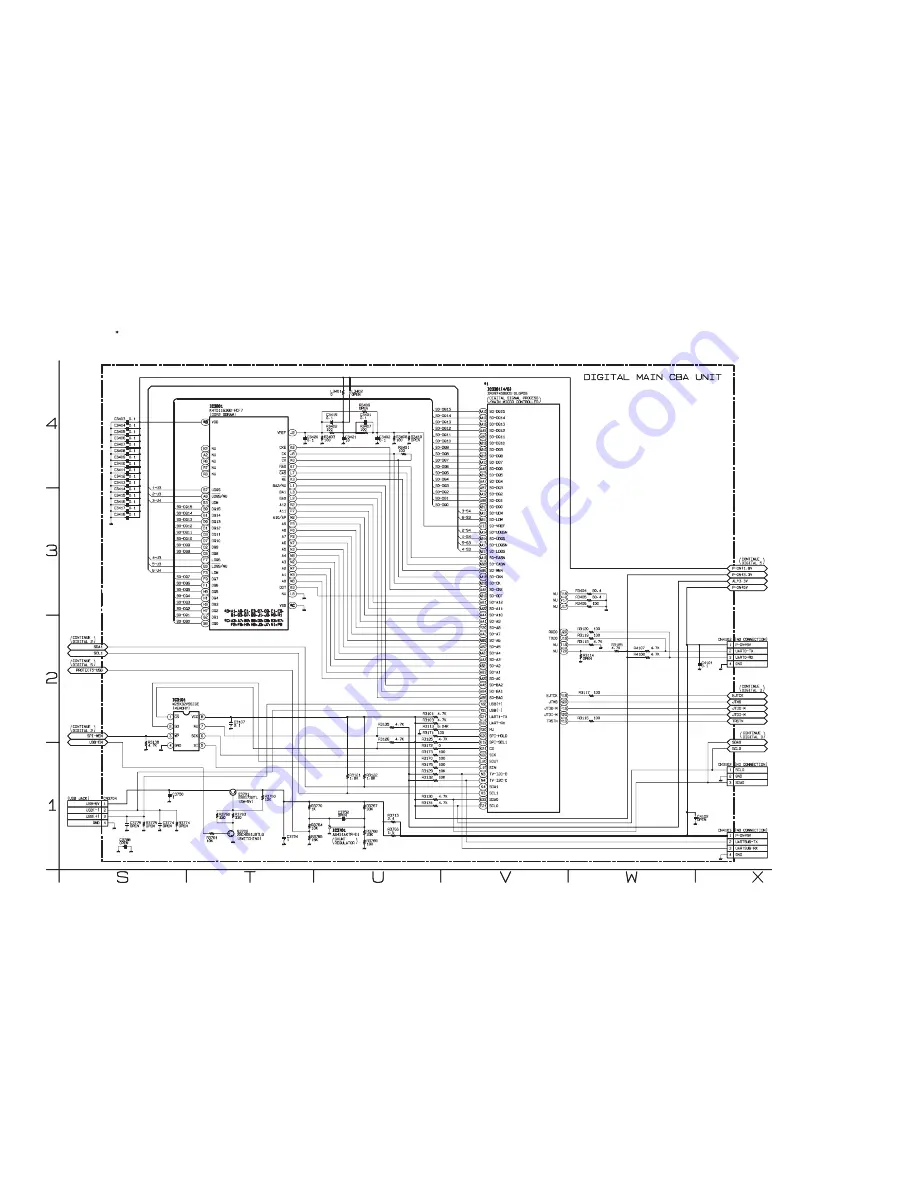
FL10.1SCD4

Digital Main 4 Schematic Diagram

The order of pins shown in this diagram is different from that of actual IC3301. 
IC3301 is divided into five and shown as IC3301 (1/6) ~ IC3301 (6/6) in this Digital Main Schematic Diagram Section.

1   NOTE:

Summary of Contents for FL10.1

Page 1: ...ange without notice Funai reserves the right to change the content herein without the obligation to notify any person or organization of such changes with the design is a registered trademark of Funai...

Page 2: ...quipment It also is important to understand that these CAUTIONS and NOTICES ARE NOT EXHAUSTIVE Funai could not possibly know evaluate and advice the service trade of all conceivable ways in which serv...

Page 3: ...net Disassembly Instructions 4 1 Electrical Adjustment Instructions 5 1 How to Initialize the LCD TV 6 1 Firmware Renewal Mode 7 1 Troubleshooting 8 1 Block Diagrams 9 1 Schematic Diagrams CBA and Tes...

Page 4: ...m dBm 76 0 76 0 76 4 Description Condition Unit Nominal Limit 1 Native Pixel Resolution Horizontal Vertical pixels pixels 1366 768 2 Brightness w filter cd m2 280 3 Viewing Angle Horizontal Vertical 8...

Page 5: ...m any AC source connect an electrical jumper across the two AC plug prongs Place the instrument AC switch in the on position Connect one lead of an ohmmeter to the AC plug prongs tied together and tou...

Page 6: ...is not isolated from the AC power line The two ground systems are electrically separated by insulation material that must not be defeated or altered 5 Observe original lead dress Take extra care to a...

Page 7: ...PVC tubing 3 Spacers 4 Insulators for transistors E When replacing AC primary side components transformers power cord etc wrap ends of wires securely about the terminals before soldering F Observe tha...

Page 8: ...exposed accessible parts RF terminals antenna terminals video and audio input and output terminals microphone jacks earphone jacks etc is lower than or equal to the specified value in the table below...

Page 9: ...he Flat Pack IC about 5 to 6 seconds Fig S 1 1 2 Remove the flat pack IC with tweezers while applying the hot air 3 Bottom of the flat pack IC is fixed with glue to the CBA when removing entire flat p...

Page 10: ...one using a sharp pin or wire to which solder will not adhere iron wire When heating the pins use a fine tip soldering iron or a hot air desoldering machine Fig S 1 4 3 Bottom of the flat pack IC is...

Page 11: ...g S 1 6 Note When using a soldering iron care must be taken to ensure that the flat pack IC is not being held by glue When the flat pack IC is removed from the CBA handle it gently because it may be d...

Page 12: ...d to remove any static electricity that may be charged on the body 2 Ground for Workbench Be sure to place a conductive sheet or copper plate with proper grounding 1 M on the workbench or other surfac...

Page 13: ...ollowing Reference Notes in the Table Step Loc No Part Removal Fig No Remove Unhook Unlock Release Unplug Unclamp Desolder Note 1 Stand Assembly D1 3 S 1 2 Rear Cabinet D1 9 S 2 2 S 3 S 4 3 S 5 3 Jack...

Page 14: ...4 2 FL10 1DC 2 Rear Cabinet S 1 1 Stand Assembly S 2 S 2 S 5 S 2 S 4 S 3 S 2 S 2 S 2 Fig D1...

Page 15: ...t 8 Stand Holder 7 Main CBA 9 LCD Module Assembly 14 Junction A CBA 12 Junction C CBA 13 Junction B CBA 15 Function CBA 16 Front Cabinet 10 Speaker Holder 11 Speaker 3 Jack Holder D 5 Jack Holder A S...

Page 16: ...750 CN3902 CN3702 CN3701 Digital Main CBA Unit CN102 CN101 CN101A CN702 AC CORD CN302 CN701 CN861A CN861B CL861 CN301 CN101B Junction C CBA Junction A CBA Junction B CBA Function CBA To LCD Module Ass...

Page 17: ...quipment is available Test Equipment Required 1 NTSC Pattern Generator Color Bar W White Window Red Color Dot Pattern Gray Scale Monoscope Multi Burst 2 Remote control unit 3 Color Analyzer How to set...

Page 18: ...The optical receptor must be set perpendicularly to the LCD Panel surface 3 Enter the Service mode 4 Press 3 button on the remote control unit 5 Press CH X Y buttons on the remote control unit so that...

Page 19: ...5 CUTOFF Press 1 button to select COR for Red Cutoff adjustment Press 3 button to select COB for Blue Cutoff adjustment DRIVE Press 4 button to select DR for Red Drive adjustment Press 6 button to se...

Page 20: ...To put the program back at the factory default initialize the LCD TV using the following procedure 1 Turn the power on 2 Enter the service mode To cancel the service mode press button on the remote c...

Page 21: ...the power off and turn the power on again Note When the Factory Upgrade is used after restarting TV shift to initial screen menu in service mode INITIALIZED will appear on the upper right of the scre...

Page 22: ...secondary side and service it if defective After servicing replace the fuse When the output voltage fluctuates FLOW CHART NO 3 Does the photocoupler circuit on the secondary side operate normally No Y...

Page 23: ...r of Q201 Yes Check C631 D631 D668 and their periphery circuit and service it if defective P ON 7V is not output FLOW CHART NO 8 Is approximately 7V voltage supplied to the cathode of D641 Check C641...

Page 24: ...service it if defective Check Q638 Q639 P ON H2 line and their periphery circuit and service it if defective No FLOW CHART NO 13 Replace Q640 P ON 3V is not output FLOW CHART NO 11 Is approximately 3V...

Page 25: ...mately 34V voltage supplied to the collector of Q634 Yes Replace IC631 Check C636 D636 D637 and their periphery circuit and service it if defective Check Q202 Q203 D204 P ON H1 line and their peripher...

Page 26: ...e control unit Yes Replace Digital Main CBA Unit When pressing each switches SW104 SW109 do the voltage of Pin 29 of CN302 increase Yes The key operation is not functioning FLOW CHART NO 1 Are the con...

Page 27: ...nput FLOW CHART NO 4 Are the DIF signal inputted to Pin 26 28 of CN302 Yes Replace Digital Main CBA Unit or LCD Module Assembly Replace Digital Main CBA Unit or LCD Module Assembly Pin 6 S VIDEO C Pin...

Page 28: ...803 and service it if defective Are the audio L R signals outputted to Pin 1 7 of IC803 No Yes Replace IC803 No Check SP861 SP862 and their periphery circuit and service it if defective Are the audio...

Page 29: ...ctive Are the audio L R signals outputted to Pin 1 7 of IC803 No Yes Replace IC803 No Check SP861 SP862 and their periphery circuit and service it if defective Are the audio L R signals inputted to Pi...

Page 30: ...if defective No No Are the audio L R signals outputted to Pin 4 6 of IC801 Check IC801 and their periphery circuit and service it if defective No Yes Are the audio L R signals inputted to Pin 6 8 of C...

Page 31: ...Q171 K3 IC3301 MAIN MICRO CONTROLLER DIGITAL MAIN CBA UNIT CN3702 CN3702 CLKOUT 25M CLKIN 25M X3101 25MHz OSC U1 V1 CLKOUT 32K CLKIN 32K X3102 32 768kHz OSC N2 N1 PROTECT3 M2 VCOM PWM M4 PROTECT2 L3...

Page 32: ...C Y JK752 VIDEO IN S VIDEO SW IN 19 19 COM VIDEO Y IN 20 20 COM VIDEO Pb IN 18 18 COM VIDEO Pr IN 16 16 MAIN CBA TU302 DIF OUT1 11 DIF OUT2 10 TUNER UNIT IF AGC 9 CN302 CN3702 DIF OUT1 26 26 IF AGC 2...

Page 33: ...CONTROL DRIVE CN302 CN3702 AUDIO MUTE 20 20 JK841 DIGITAL AUDIO OUT COAXIAL Q841 Q771 Q722 BUFFER SPDIF 2 2 SPDIF 23 23 Q801 CONTROL LOGIC 3 10 9 13 IC803 OP AMP 1 3 7 5 DRIVE AUDIO L AUDIO R TO DIGIT...

Page 34: ...7 26 27 23 24 20 21 17 18 8 7 11 10 14 13 5 4 1 2 9 4 6 1 3 10 12 16 15 7 9 4 6 1 3 10 12 16 15 JK3702 TMDS D0 TMDS D0 TMDS D1 TMDS D1 TMDS D2 TMDS D2 TMDS CLOCK TMDS CLOCK SDA SCL TMDS CLOCK TMDS CLO...

Page 35: ...TROL SWITCH CURRENT CONTROL SWITCH Q1700 CURRENT CONTROL SWITCH OVER VOLTAGE PROTECTOR OVER VOLTAGE PROTECTOR OVER VOLTAGE PROTECTOR OVER VOLTAGE PROTECTOR Q1550 OVER VOLTAGE PROTECTOR Q1551 OVER VOLT...

Page 36: ...V P ON 7V AL 3 3V P ON 3 3V P ON 5V LCD MODULE ASSEMBLY DIGITAL MAIN CBA UNIT PANEL 7 1V 8 P ON 3 3V 19 20 P ON 3 3V 6 7 PANEL 24 5V 4 PANEL 13V 2 3 AL 3 3V 21 22 16 10 P ON 7V 16 P ON 3V 10 P ON 5V 1...

Page 37: ...k fire or other hazards Notes 1 Do not use the part number shown on these drawings for ordering The correct part number is shown in the parts list and may be slightly different or amended since these...

Page 38: ...mended since the drawings were prepared 2 To maintain original function and reliability of repaired units use only original replacement parts which are listed with their part numbers in the parts list...

Page 39: ...10 3 FL10 1SCM1 Main 1 Schematic Diagram...

Page 40: ...10 4 FL10 1SCM2 Main 2 Schematic Diagram...

Page 41: ...10 5 FL10 1SCM3 Main 3 Junction B Schematic Diagram...

Page 42: ...fuse CAUTION ATTENTION Utiliser un fusible de rechange de m me type de 4A 125V 4A 125V CAUTION Fixed voltage or Auto voltage selectable power supply circuit is used in this unit If Main Fuse F601 is b...

Page 43: ...10 7 FL10 1SCJ Jack Junction C Schematic Diagram...

Page 44: ...10 8 FL10 1SCF Function Junction A Schematic Diagram...

Page 45: ...Main 1 Schematic Diagram The order of pins shown in this diagram is different from that of actual IC3301 IC3301 is divided into five and shown as IC3301 1 6 IC3301 6 6 in this Digital Main Schematic...
Page 46: ...l Main 2 Schematic Diagram The order of pins shown in this diagram is different from that of actual IC3301 IC3301 is divided into five and shown as IC3301 1 6 IC3301 6 6 in this Digital Main Schematic...

Page 47: ...l Main 3 Schematic Diagram The order of pins shown in this diagram is different from that of actual IC3301 IC3301 is divided into five and shown as IC3301 1 6 IC3301 6 6 in this Digital Main Schematic...

Page 48: ...l Main 4 Schematic Diagram The order of pins shown in this diagram is different from that of actual IC3301 IC3301 is divided into five and shown as IC3301 1 6 IC3301 6 6 in this Digital Main Schematic...

Page 49: ...l Main 5 Schematic Diagram The order of pins shown in this diagram is different from that of actual IC3301 IC3301 is divided into five and shown as IC3301 1 6 IC3301 6 6 in this Digital Main Schematic...

Page 50: ...hematic Diagram FL10 1SCD6 The order of pins shown in this diagram is different from that of actual IC3301 IC3301 is divided into five and shown as IC3301 1 6 IC3301 6 6 in this Digital Main Schematic...

Page 51: ...D666 INV 31V J040 D668 D1010 INV 31V J041 2 1 29 28 CN301 D1011 INV 31V J042 2 1 29 28 CN302 D1012 GND J043 1 2 29 28 CN303 D1013 GND J044 J045 J046 R1012 GND J047 D670 DRIVE 12 5V J048 J049 D1401 D14...

Page 52: ...D1664 Q201 D1665 Q202 D1667 Q203 Q205 Q206 Q207 Q208 Q209 D301 D302 D303 D304 Q401 Q402 Q211 Q215 Q601 Q602 JS1001 JS1002 JS1004 JS1005 Q801 L601 D901 D902 D903 D904 D905 D906 D907 D908 BC601 L804 M...

Page 53: ...8 5 2 J 8 0 1 J 8 0 2 J 8 0 4 J 8 0 5 J 8 0 6 J 8 0 7 J 8 0 8 J 8 1 0 J 8 1 2 J 8 1 3 J 8 1 4 J K 7 1 1 J 8 1 5 J 8 1 6 J 8 1 7 J 8 1 8 J 8 1 9 Q 7 7 1 Q 7 2 2 Q 7 7 3 J 8 2 0 Q 7 7 4 J 8 2 1 C N 7 0...

Page 54: ...8 4 1 J K 7 2 2 J K 7 2 1 J 8 1 1 J 8 2 2 G N D D 7 0 9 D 7 0 6 D 7 0 5 P O N 9 V P O N 9 V A M P R S P C N 8 6 1 B C L 8 6 1 C N 8 6 2 B C L 8 6 2 P b P b P b C 1 1 1 C 1 0 4 R 1 1 0 R 1 0 7 C 1 0 6...

Page 55: ...veform check points Shown in Schematic Diagram CVBS 0 2V 20 s WF1 Pin 4 of CN302 S VIDEO Y 0 2V WF2 Pin 8 of CN302 20 s S VIDEO C 0 2V WF3 Pin 6 of CN302 20 s AUDIO 0 1V 0 5ms WF7 Pin 13 of CN302 VIDE...

Page 56: ...3701 CN301 23 19 21 15 17 22 20 18 16 14 10 12 6 8 13 11 9 7 5 1 3 4 1 5 3 9 7 2 4 6 8 10 14 12 18 16 11 13 15 17 19 23 21 20 2 P ON H2 AUDIO L OUT NU GND AUDIO R OUT NU PROTECT3 AMP L OUT GND AMP R O...

Page 57: ...01 Function CBA SP861 SP862 Main CBA B8 A3 Stand Assembly Jack CBA L2 L2 B3 B3 L1 L1 L17 B13 L13 B14 B2 S5 L3 B44 B7 B7 L12 L12 L12 L3 L3 L11 A4 LCD1 L9 L9 L3 L4 L4 L3 L3 A10 L1 L1 L8 B8 L1 L3 L3 L3 J...

Page 58: ...13 2 FL10 1PEX Packing S3 S1 Tape Packing Tape Packing Tape Packing Tape Packing Tape S2 S3 X1 Some Ref Numbers are not in sequence L17 X2 S4 X8 X6 S6 S5 Stand Assembly X4 X3 FRONT FRONT Tape...

Page 59: ...01 WIRE ASSEMBLY 29PIN FFC 29PIN 50MM WX1A94F0 101 CL3701 WIRE ASSEMBLY 29PIN FFC 29PIN 50MM WX1A94F0 101 CL3702 WIRE ASSEMBLY 29PIN FFC 29PIN 70MM WX1A94F0 111 CL3902 WIRE ASSEMBLY 24PIN FFC 24PIN 80...

Page 60: ...M CE1EMZNDL102 C645 POLYESTER FILM CAP PB FREE 0 0022 F 100V J CA2A222DT018 C647 ELECTROLYTIC CAP 100 F 10V M H7 CE1AMAVSL101 C649 ELECTROLYTIC CAP 220 F 10V M H7 CE1AMAVSL221 C650 ELECTROLYTIC CAP 22...

Page 61: ...DE ZENER 5V6BSB T26 NDTB5R6BST26 D210 SWITCHING DIODE 1SS133 T 77 QDTZ001SS133 D211 SWITCHING DIODE 1SS133 T 77 QDTZ001SS133 D212 SWITCHING DIODE 1SS133 T 77 QDTZ001SS133 D303 DIODE ZENER 5V6BSB T26 N...

Page 62: ...T 77 QDTZ001SS133 D1762 SWITCHING DIODE 1SS133 T 77 QDTZ001SS133 D1763 SWITCHING DIODE 1SS133 T 77 QDTZ001SS133 D1764 SWITCHING DIODE 1SS133 T 77 QDTZ001SS133 D1765 SWITCHING DIODE 1SS133 T 77 QDTZ00...

Page 63: ...2 2k RRXAJR5Z0222 Ref No Description Part No R411 CHIP RES 1 10W J 22k RRXAJR5Z0223 R412 CHIP RES 1 10W J 22k RRXAJR5Z0223 R413 CHIP RES 1 10W J 22k RRXAJR5Z0223 R601 GLASS GLAZE RES 1 2W J 1M RXX2JZ...

Page 64: ...R1037 CHIP RES 1608 1 10W 0 RRXAZR5Z0000 R1043 CHIP RES 1 10W J 12k RRXAJR5Z0123 Ref No Description Part No R1044 CHIP RES 1 10W F 2 7k RRXAFR5H2701 R1045 CHIP RES 1 10W F 1 2k RRXAFR5H1201 R1048 RES...

Page 65: ...ER HVT 179 LTZ3PZ0XB012 T1600 TRANS INVERTER HVT 179 LTZ3PZ0XB012 T1700 TRANS INVERTER HVT 179 LTZ3PZ0XB012 TU302 TUNER UNIT ATSC TDAU4 D05A UTNATS0AL002 Ref No Description Part No Ref No Description...

Page 66: ...CHIP RES 1 10W J 2 2k RRXAJR5Z0222 R797 CHIP RES 1 10W J 2 2k RRXAJR5Z0222 R843 CHIP RES 1 10W J 110 RRXAJR5Z0111 R844 CHIP RES 1 10W J 220 RRXAJR5Z0221 R845 CHIP RES 1 10W J 100k RRXAJR5Z0104 Ref No...

Page 67: ...BLY 8PIN 8PIN 150MM WX1A9170 001 Ref No Description Part No JUNCTION B CBA MJC D Consists of the following CONNECTOR CN862B 242SERIESCONNECTORTUC P04X B1WHT ST JCTUB04TG002 MISCELLANEOUS CL862 WIRE AS...

Page 68: ...servicing NOTE Parts that are not assigned part numbers are not available Different parts from the original model LC220SS1 Ref No Description Part No A1 FRONT CABINET A0175UH 1EM025433 A3 CONTROL PLAT...

Page 69: ...replacing any of these components read carefully the product safety notice in this service manual Don t degrade the safety of the product through improper servicing NOTE Parts that are not assigned pa...

Page 70: ...s that are not assigned part numbers are not available Different parts from the original model LC220SS1 Ref No Description Part No A1 FRONT CABINET A0173UH 1EM124953 A3 CONTROL PLATE A91N3UH 1EM325763...

Page 71: ...replacing any of these components read carefully the product safety notice in this service manual Don t degrade the safety of the product through improper servicing NOTE Parts that are not assigned pa...

Page 72: ...15 1 FL10 1REV REVISION HISTORY Chassis FL10 1 2010 03 30 LC220SS1 added 2010 04 23 LC220EM1 added 2010 05 06 LC220SL1 added TBD 22MF330B F7 added...

Reviews: