Reproduction forbidden without Fibocom Wireless Inc. written authorization - All
rights reserved.
FIBOCOM SC138-
NA
Series Hardware Guide
71/88
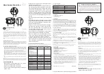
4 RF PCB Layout Design Guide
For user PCB, the characteristic impedance of all RF signal lines shall be controlled at 50 Ω. In general,
the impedance of the RF signal line is determined by the dielectric constant of the material, the routing
width (W), the ground clearance (S), and the height of the reference ground plane (H). The characteristic
impedance of PCB is usually controlled by microstrip line and coplanar waveguide. In order to reflect the
design principle, the following figure displays the structure design of microstrip line and coplanar
waveguide when the impedance line is controlled at 50 Ω.
Complete structure of microstrip line
Figure 4-1 Microstrip line structure of two-layer of PCB
Complete structure of coplanar waveguide
Figure 4-2 Coplanar waveguide structure of two-layer PCB