GPS-RECEIVER JP7-T
VERSION 1.02
10 First steps to make it work
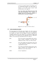
Figure 16
:
The minimum hardware interface of JP7-T to get started.
-
Antenna
: The antenna connection is the most critical part of PCB
routing. Previously placing the JP7-T on the PCB secure that
the connection to the antenna signals is routed. In order to
make it properly functional a control impedance line has to
connect the RF_IN signal with antenna feed points or antenna
connector, respectively. The routing on the PCB depends on
your choice.
-
Power:
The input power is also very important as far as the minimum
and maximum voltage is concerned. The power supply of JP7-
T family has to be a single voltage source of VCC at 3.3 VDC.
The power supply has to be able to provide a sufficient current
which typically rises to 200 mA. Please, connect GND pins to
ground, and connect the line which supply the VCC pin to +3.3
V, properly. If they are correctly connected, a proper RESET
signal is internally generated the board is full powered and the
unit begins obtaining its position fix.
-
Serial Interface:
The JP7-T family
provides two serial interfaces. Each
interface is provided with two-wire the SDI1, SDO1 supports
line and ground for the first serial interface (port A) and SDI2,
SDO2 supports line and ground for the second serial interface
(port B). These pins are both 3.3 V CMOS and 5 V TTL
compatible. In order to use different voltage levels, a
appropriate level shifters has to be used.
E. g. in order to provide RS232 compatible levels use the 3 V
compatible MAX3232 transceiver from Maxim or others based
on the required levels. The GPS data will be transmitted
through port A (first serial port), if an active antenna is
connected, which has a good view to sky (no obstacle). You
This confidential document is the property of FALCOM GmbH and may not be copied or circulated without permission.
Page 45


