GPS-RECEIVER JP7-T
VERSION 1.02
is confidential document is the property of FALCOM GmbH and may
not be copied or circulated without permission.
Page 25
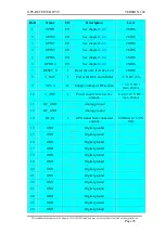
Pin
Name
I/O
Description
Level
18
RF_GND
Analog ground
19
V_ANT
I
Power supply for active antenna
upto +12 V DC
20
VC3.0
O
Supply voltage of RF section
+3.0 V DC
21
V_BAT
I
Power for RTC and SRAM
+3 V DC ±5%
22
RESET_N
I
Resets the unit if active LOW
CMOS
23
GPIO10
I/O
See chapter
CMOS
24
GPIO6
I/O
See chapter
CMOS
25
GPIO5
I/O
See chapter
CMOS
26
GPIO7
I/O
See chapter
CMOS
27
GPIO0
I/O
See chapter
CMOS
28
GPIO1
I/O
See chapter
CMOS
29
T-MARK
O
One pulse per second
CMOS
30
GND
Digital ground
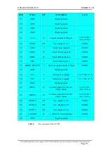
Table 4:
Pin assignment of the JP7-T
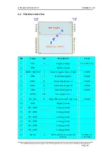
6.7 Balls assignment of the JP7-TB
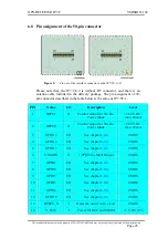
Figure 4:
Balls assignment of the JP7-TB
Th


