


Description
GPS receiver
A2D–JP
Version 1.03
Side 25
❐
Initialised start:
is if last known position (in EEPROM) and
time are available. Satellite data validity has expired.
❐
Cold start:
means only almanac information is used.
❐
Frozen start:
no valid internal data source available.
Built in test (BIT) mode
A BIT is available on command from the application software using
binary Message 1300. The BIT is used to provide a health status of
the GPS receiver functions. Results of the BIT are available in binary
Message 1100. A BIT command is possible in NMEA protocol, too.
Power modes and power sequencing requirements
The GPS receiver have three power modes: Off, Operate, and
„Keep-Alive“.
The Off mode assumes that neither main power is available.
In the Operate mode the GPS receiver's components are full supp-
lied at 3,3 VDC. The M_RST control signal is at a "high" logic level.
From Operate mode, the GPS receiver will enter a "Keep Alive"
mode when supply voltage is available at the VBATT signal input
and VC3 voltage is removed. VBATT provides power for SRAM and
RTC.
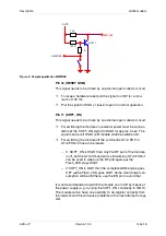
6.3.2 Hardware interface
The following paragraphs describe the basic functions allocated to
the various pins on the AMP interface connector. These functions
are divided into three groups: Configuration and timing signals, se-
rial communication signals, and DC input signals.
6.3.2.1 Configuration and timing signals
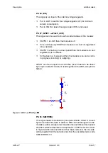
Pin 55: Master reset (M_RST)
This signal allows the OEM to generate a system hardware reset to
the GPS receiver. This signal is capable of being driven directly by
an external microprocessor or by external logic without the need for
any external pull-up or pull-down resistors. The OEM can generate a
system reset to the GPS receiver by pulling the M_RST control si-
gnal low to ground.
This signal can also be used to provide control of the GPS receiver's
Operate mode without removing prime input power from the GPS re-
ceiver. When M_RST is pulled to ground, the GPS receiver will enter
a low power state for as long as the M_RST signal is asserted low.
The M_RST signal must be pulled to a CMOS logic „high“ level coincident
with, or after, the application of prime DC power for the receiver to enter its
Operate mode. The M_RST must be held at ground level for a minimum of
150 nanoseconds to assure proper generation of a hardware reset to the
receiver.


