SED1520 Series
EPSON
2–7
SED1520
Series
(3) LCD Drive Circuit Signals
Name
Description
CL
Input. Effective for an external clock operation model only.
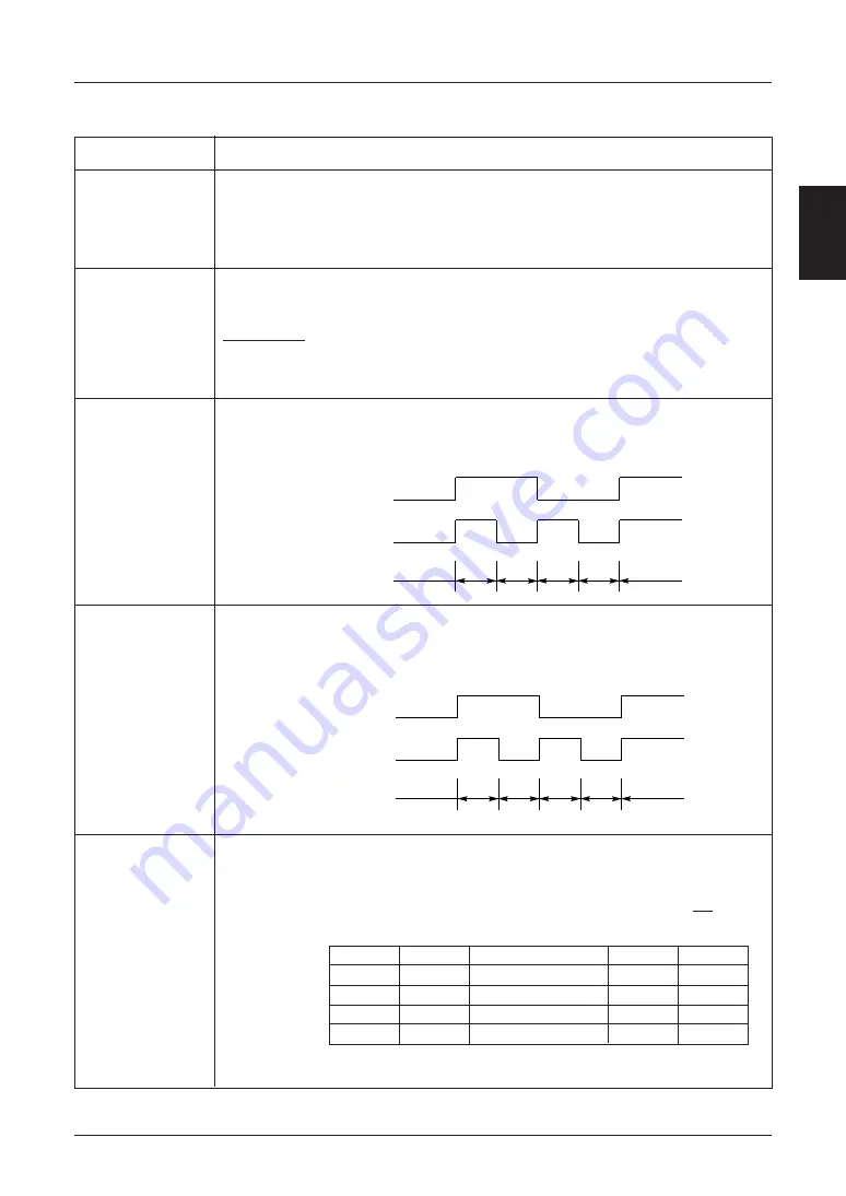
This is a display data latch signal to count up the line counter and common counter
at each signal falling and rising edges. If the system has a built-in oscillator, this is
used as an output pin of the oscillator amp and an Rf oscillator resistor is con-
nected to it.
FR
Input/output.
This is an I/P pin of LCD AC signals, and connected to the M terminal of common
driver.
I/O selection
• Common oscillator built-in model:
Output if M/S is 1;
Input if M/S is 0.
• Dedicate segment model:
Input
SEGn
Output.
The output pin for LCD column (segment) driving. A single level of V
DD
, V
2
, V
3
and
V
5
is selected by the combination of display RAM contents and RF signal.
1
0
1
0
1
0
V
V2
V5
V3
DD
FR signal
Data
Output level
COMn
Output.
The output pin for LCD common (low) driving. A single level of V
DD
, V
1
, V
4
and V
5
is selected by the combination of common counter output and RF signal. The
slave LSI has the reverse common output scan sequence than the master LSI.
1
0
1
0
1
0
V
V1
V5
V4
DD
FR signal
Counter output
Output level
M/S
Input.
The master or slave LSI operation select pin for the SED1520 or SED1522.
Connected to V
DD
(to select the master LSI operation mode) or V
SS
(to select the
slave LSI operation mode).
When this M/S pin is set, the functions of FR, COM0 to COM15, OSC1 (CS), and
OSC2 (CL) pins are changed.
* The slave driver has the reverse common output scan sequence than the master
driver.
M/S
FR
COM output
OSC1
OSC2
SED1520F
0A
V
DD
Output
COM0 to COM15
Input
Output
V
SS
Input
COM31 to COM16
NC
Input
SED1522F
0A
V
DD
Output
COM0 to COM7
Input
Output
V
SS
Input
COM15 to COM8
NC
Input


