08. APPLIED CIRCUIT EXAMPLES
20
EPSON
S1F76640 Technical Manual (Rev.1.5)
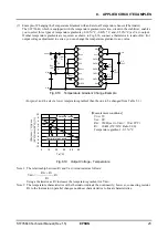
Note 1: <Notes on load connection>
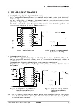
As shown in Fig.8.8, when connecting load between V
SS
in the first stage (or other voltage below V
SS
in the second stage) and V
REG
in the second stage in serial connection, the following points should be
noted: When the IC is activated or no normal output is generated at the V
REG
pin while V
REG
is turned
off by the P
OFF
signal, current flows into to the V
REG
pin from V
SS
in the first stage (or other voltage
below V
SS
in the second stage) through load. If the voltage exceeding the absolute maximum rating
below V
SS
in the second stage is generated at the V
REG
pin, the may interfere with normal operation of
the IC. For serial connection, as shown in Fig.8.8, connect diode D1 between V
DD
in the second stage
and V
REG
, so that the voltage below V
SS
in the second stage will not be applied to the V
REG
pin.
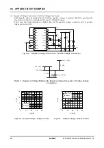
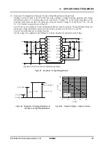
Note 2: In Fig.8.8, the first stage is assigned to triple boosting and the next-stage to quadruple boosting;
however, quadruple boosting is available for both the first and next stages unless the input voltage
V
DD
’ - V
SS
’ in the next stage exceeds the standard value (6.0V). For serial connection, each IC must be
designed in compliance with the standard (V
DD
- V
SS
≤
6.0V, V
O
- V
SS
≤
24V) (See Fig.8.9).
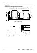
Note 3: When double boosting is provided in the first stage, the first-stage CAP1- output can be used as a
next-stage clock; however, when triple boosting is provided, it cannot be used as a next-stage clock.
Therefore, to obtain a next-stage clock, externally install R
OSC
and use an internal oscillator. As shown
in Table 4.2, the next-stage external clock operation by the pre-stage CAP1- output is available only for
temperature gradient CT = -0.5%/
°
C. If another temperature gradient is required, use an internal
oscillator like the above.
Note 4: In serial connection, the temperature gradient is provided for the V
SS
- V
REG
voltage (V
REG
– V
SS
’ in
Fig.8.9) of the IC in which the stabilizer is active.
The V
REG
value changes according to temperature as follows:
It changes at the ratio above.
Δ
|
V
REG
|
CT ( V
REG
(25
°
C) - V
SS
’ )
Δ
T

