

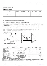


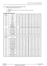

10. Interface timing when power ON / OFF
RX4111CE
Jump to
ETM62E-02
Seiko Epson Corporation
14
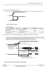
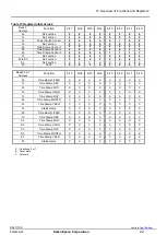
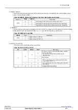
10.2. V
DD
and CE Timing at Power On
When the power is turned to ON, use with CE
=
Low,
”
V
CL
V in the diagram
”
as illustrated in the following timing chart.
V
DD
1.6 V
V
CL
t
CL
CE
Figure 15 VDD, CE sequence
Table 10 CE Timing
Item
Symbol
Condition
Specification
Unit
CE voltage when power is
turned to ON
V
CL
CE impressed voltage
until V
DD
=
1.6 V
0.3 Max.
V
CE = V
CL
V time when power
is turned to ON
t
CL
Time to maintain CE = V
CL
until V
DD
=
1.6 V
40 Min.
ms
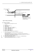
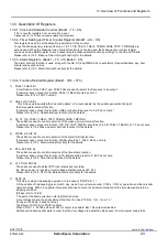
10.2. Restrictions on Access Operations During Power-on Initialization and Recovery from Backup
Because most of RTC registers are synchronized with the oscillation clock of the built-in crystal oscillator, the RTC does
not work normally without the integrated oscillator having stabilized. Please initialize the RTC at the time the power supply
voltage returns (VLF = 1) after the oscillation has stabilized (after oscillation start time t_
STA
).
If intending to access the RTC after the main supply voltage returns, please note following points:
V
DD
V
DD
detect vV
DET
Internal oscillation
(illustration)
t
_str
Oscillation start time
(internal oscillation wait time)
Access is enabled
Normal operation start
Minimum voltage for clock maintenance V
CLK
During power-on initialization or power
supply voltage recovery after drop in clock
maintenance voltage
30
[ms]
After 30 ms progress, Confirm a state by VLF-bit
At the time of VLF=1: After a t_str wait, initial setting is necessary.
At the time of VLF=0: Register access is possible.
V
BAT
FOUT
Figure 16 Oscillation start time chart (Power initial supply)