E0C88832/88862 TECHNICAL MANUAL
EPSON
29
5 PERIPHERAL CIRCUITS AND THEIR OPERATION (Oscillation Circuits and Operating Mode)
When crystal oscillation is selected, a crystal
oscillation circuit can be easily formed by connect-
ing a crystal oscillator X'tal1 (Typ. 32.768 kHz)
between the OSC1 and OSC2 terminals along with
a trimmer capacitor C
G1
(5–25 pF) between the
OSC1 terminal and V
SS
.
In addition, the gate capacitor C
G1
(15 pF) can be
built into the circuit by the mask option.
When CR oscillation is selected, connect a resistor
(R
CR1
) between the OSC1 and OSC2 terminals.
When external input is selected, release the OSC2
terminal and input the rectangular wave clock into
the OSC1 terminal.
5.3.4 OSC3 oscillation circuit
The OSC3 oscillation circuit generates the system
clock when the CPU and some peripheral circuits
(output port, serial interface and programmable
timer) are in high speed operation.
This oscillation circuit stops when the SLP instruc-
tion is executed, or the OSCC register is set to "0".
In terms of oscillation circuit types, any one of
crystal oscillation, ceramic oscillation, CR oscilla-
tion or external clock input can be selected with the
mask option.
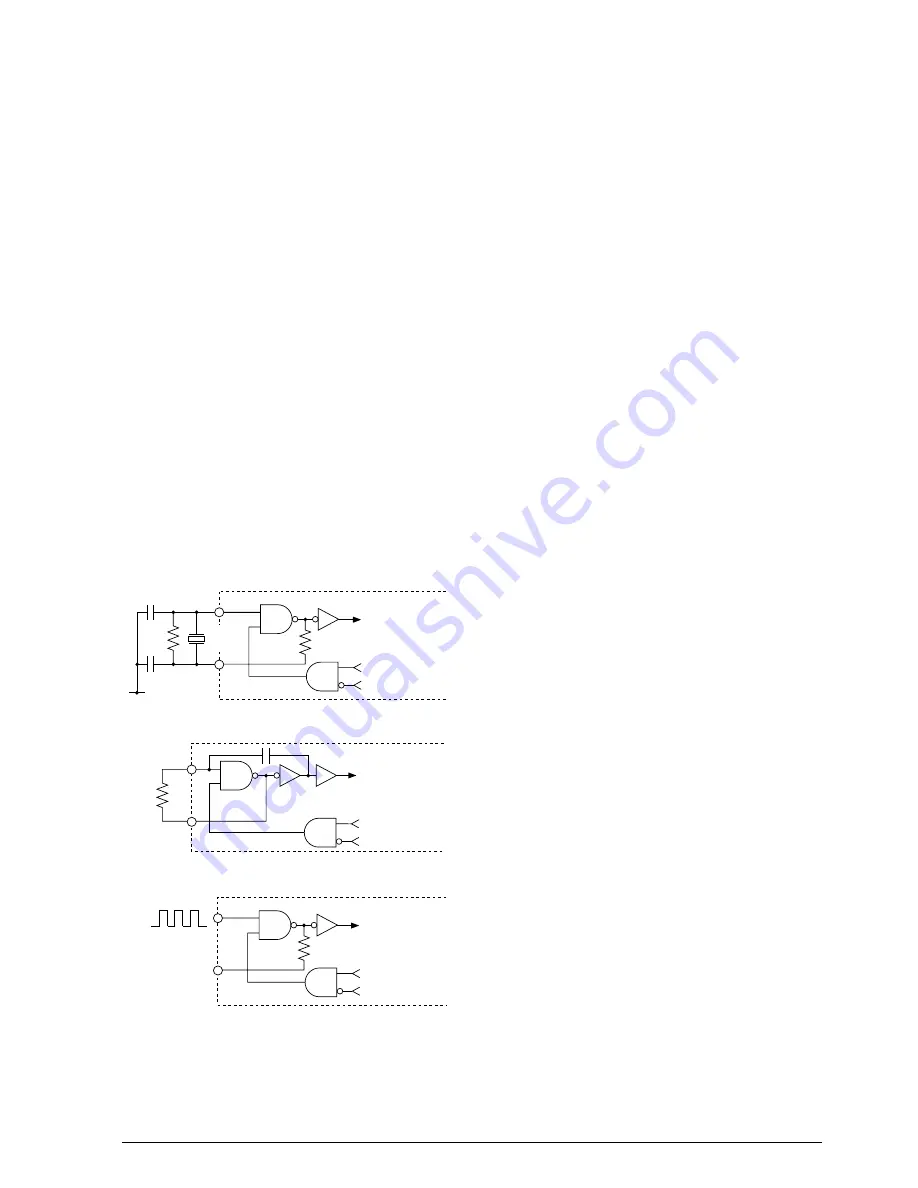
Figure 5.3.4.1 shows the configuration of the OSC3
oscillation circuit.
When crystal or ceramic oscillation circuit is
selected, the crystal or ceramic oscillation circuit are
formed by connecting either a crystal oscillator
(X'tal2) or a combination of ceramic oscillator
(Ceramic) and feedback resistor (Rf) between OSC3
and OSC4 terminals and connecting two capacitors
(C
G2
, C
D2
) between the OSC3 terminal and V
SS
, and
between the OSC4 terminal and V
SS
, respectively.
When CR oscillation is selected, the CR oscillation
circuit is formed merely by connecting a resistor
(R
CR3
) between OSC3 and OSC4 terminals.
When external input is selected, release the OSC4
terminal and input the rectangular wave clock into
the OSC3 terminal.
5.3.5 Operating mode
You can select three types of operating modes using
software, to obtain a stable operation and good
characteristics (operating frequency and current
consumption) over a broad operation voltage. Here
below are indicated the features of the respective
modes.
•
Normal mode (V
DD
= 2.4 V–5.5 V)
This mode is set following the initial reset. It
permits the OSC3 oscillation circuit (Max. 4.2
MHz) to be used and also permits relative low
power operation.
•
Low power mode (V
DD
= 1.8 V–3.5 V)
This is a lower power mode than the normal
mode. It makes ultra-low power consumption
possible by operation on the OSC1 oscillation
circuit, although the OSC3 circuit cannot be used.
•
High speed mode (V
DD
= 3.5 V–5.5 V)
This mode permits higher speed operation than
the normal mode. Since the OSC3 oscillation
circuit (Max. 8.2 MHz) can be used, you should
use this mode, when you require operation at 4.2
MHz or more. However, the current consump-
tion will increase relative to the normal mode.
Using software to switch over among the above
three modes to meet your actual usage circum-
stances will make possible a low power system. For
example, you will be able to reduce current con-
sumption by switching over to the normal mode
when using the OSC3 as the CPU clock and,
conversely, changing over to the low power mode
when using the OSC1 as the CPU clock (OSC3
oscillation circuit is OFF).
Note: Do not turn the OSC3 oscillation circuit ON in
the low power mode. Do not switch over the
operating mode (normal mode ´ high speed
mode) in the OSC3 oscillation circuit ON
status, as this will cause faulty operation.
You can not use two modes, the low power
mode and the high speed mode on one
application, with respect to the operating
voltages.
V
SS
OSC4
OSC3
Rf
C
D2
C
G2
f
OSC3
Oscillation circuit
control signal
SLEEP status
X'tal 2
or
Ceramic
Oscillation circuit
control signal
SLEEP status
OSC4
OSC3
R
CR3
f
OSC3
OSC4
OSC3
External
clock
N.C.
V
SS
V
DD
f
OSC3
Oscillation circuit
control signal
SLEEP status
(1) Crystal/Ceramic oscillation circuit
(2) CR oscillation circuit
(3) External clock input
Fig. 5.3.4.1 OSC3 oscillation circuit
Summary of Contents for 0C88832
Page 6: ......


