ISL55180 EVM Getting Started
Rev A04: 11/28/2012
Copyright
Elevate Semiconductor Corporation 2012
Page 19 of 20
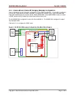
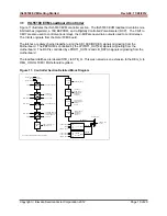
3.1 ISL55180 EVM Loadboard Controller
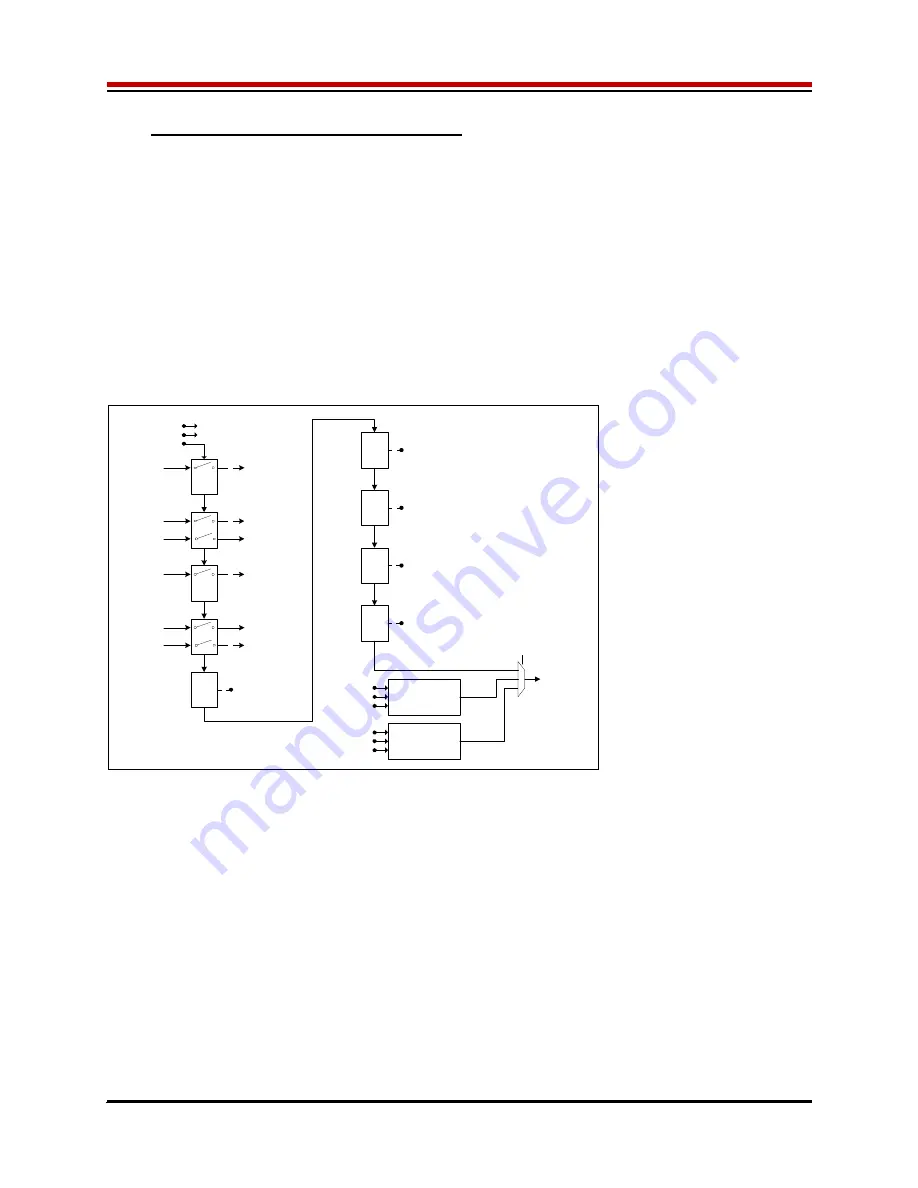
Figure 11 illustrates the ISL55180 EVM controller section. The ISL55180 EVM loadboard contains nine
8-bit latches (registers), a 16K EEPROM, and a Digitally Controlled Potentiometer (DCP). The Cbit1 to
CBit7 are also used to control various relays, the C-Bit# are open-drain outputs used to control relays.
The C-Bits originate from the Octal FVMI board.
The latches are daisy chained together using the SDI_SCK/RCK/CS signals originating from the
Motherboard. The EEPROM is controlled by the LPORT1_OUT[4:2] signals originating from the
motherboard. The DCP is controlled by LPORT1_OUT4/2 and LB_DATA3 signals originating from the
motherboard.
The loadboard latches are labeled STB_I to STB_Q. This was named as an extension to the REG_A to
REG_H Octal FVMI / Motherboard registers.
Figure 11: Controller Section Detailed Block Diagram
EEPROM
1K x 16-Bit
Latch
N
8
DUTGND#_SEL (8)
Latch
O
8
LB_AMUX (4)
GANG_IN_SEL
DUTGND_SEL
REXT_SEL
VREF_SEL
Latch
P
8
LB_AMUX_EN0
RDB_SEL[2:0] (3)
FSEL (3)
Unused
Switch I
GND
8
CON_FORCE#_TN
Switch J
GND
7
LPORT1_OUT3
CLK
CS
DIN
LPORT1_OUT2
LPORT1_OUT4
EEPROM_DO
LPORT1_OUT3
SCK
RCK / CS
TC_21
Latch
Q
RB_SER_DO
LPORT3_IN2
(to PC)
RDB_SEL[2:0]
DOUT
Unused (6)
CON_EF_TN
8
GANG#_SEL (4)
TESTP_SEL
TESTN_SEL
Unused (2)
LPORT1_OUT4
TEST_NODE
CON_ES_TN
Latch
M
8
CENT_[D:A]_SEL (4)
CENT_D[3:0] (4)
Switch
K
8
CON_SENSE#_TN
TEST_NODE
Switch L
GND
CON_MON_REF_TN
CON_MONITOR_TN
CON_MI_MON_TN
TEST_NODE
5
Unused (5)
DCP
LPORT1_OUT3
CLK
CS*
DIN
CBIT3
LPORT1_OUT4
DOUT
DCP_DO
Only showing Europa/Switcher loadboard mapping

