background image

-61-

Troubleshooting

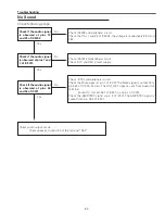
No Power

Lamp Cover switch

Make sure that the lamp cover is mounted correctly. If not or  

the  lamp  cover  removed,  the  lamp  does  not  light  on  for  the 

safety. Check the lamp cover and lamp cover switch (SW902).

-  

When all of LED indicators are not lighting

,  the symptom indicates that the primary power supply circuit does 

not operate properly. Check the power primary circuit and parts as follow;


AC cord, F601 (Fuse), Power board,


SW601 (Thermal sw.)  short in normal


 SW601 opens when the surrounding temperature of the switch exceeds 85°C.

This projector provides a function which can be specified a defective area simply by indicating the LEDs. Connect the 

AC cord and press the Power button once and then check the LED indication.

 When the WARNING (red)  and POWER (red) indicators are blinking

, the symptom indicates that the projec-

tor detected an abnormal temperature risen inside the projector. Check the air filters and remove the object near 

the intake and exhaust fan openings, and wait until the POWER indicator stops blinking, and then try to turn on 

the projector. 


 The internal temperature is monitored by sensor ICs, IC8831, IC8821 on the Main board and IC8811 on the 

R/C board.

  When the WARNING indicator lights red

, the symptom indicates that the projector detected an abnormality in 

the cooling fan operation or in the power supply secondary circuits. Check fan operation and power supply lines, 

and the driving signal status.

 The P_FAIL signal (Error: L) is sent to pin 215  of IC301<SCALER> when the abnormality occurred inside the 

projector, and then the IC301 sends the shutdown signal, LAMP_DC_ON, to the power supply circuit to stop its 

operation, and signal LAMP_SCI to the lamp ballast board via IC4891 and SW902<lamp cover switch> to stop 

operation of the lamp circuit. 

An abnormality occurs on the secondary power supply;


 Check power supplies S16V, S6V, S-7V. P_FAIL signal becomes “Low” when the abnormality occurs on 

any of the power supply lines.

An abnormality occurs on the fan control circuit;


Check FN001, FN002, FN003, FN004, FN005 and peripheral circuit.


 If  any  of  the  fans  has  an  error,  the  fan  lock  signal  drives  Q3601  becomes  "High". As  the  result,  signal 

FAN_ERR becomes Low and is sent to lamp ballast board to stop lamp circuit. 

An abnormality occurs on the drive signals;


 ON_150V signal (Power-on: H) is output from pin 95 of IC301 and switches IC592,15.5VL supply circuit, 

         ON_33V signal (Power-on: H) is output from pin 188 of IC301 and switches IC5621, 1.0V and Q3582 33V   

         supply circuit. 


 LAMP_DC_ON signal (Power-on: H)  is output from pin 89 of IC301 and supplied to the P.C Control IC, 

IC621, on the power supply board through Q691, and PC663.


LAMP_SCI signal (Power-on: H) is output from pin 14 of IC9885 and applied to pin 2 of IC4891 and out 

         put pin 4 and then supplied to the lamp ballast board through SW902<Lamp Cover SW>. 


 LAMP_DET signal at the pin 285 of IC301 is applied from the lamp ballast unit. If the abnormality occurred 

on the lamp ballast unit, LAMP_DET signal becomes “High” and then IC301 shuts down the power supply 

circuit.

Summary of Contents for LC-XBM31

Page 1: ...parts identified in this manual are available through Eiki s normal distribution chan nels In addition to service part number the generic descriptions have been given where possible to allow your ser...

Page 2: ...ndenser Out lens adjustment 27 Relay lens Out adjustment 28 Electrical Adjustments 29 Service Adjustment Menu Operation 29 Circuit Adjustments 30 Test Points and Locations 35 Service Adjustment Data T...

Page 3: ...solated COLD from AC line by using the converter transformer Primary side of the converter and lamp power supply unit circuit is connected to the AC line and it is hot which hot circuit is identified...

Page 4: ...ing Frequency H sync 15 kHz 100 kHz V sync 50 100 Hz Optical Information Projection Image Size Diagonal Adjustable from 40 to 300 Throw Distance 3 6 34 4 1 1m 10 5m Projection Lens F 2 0 2 15 lens wit...

Page 5: ...ector provides the following circuit protections to operate in safety If the abnormality occurs inside the pro jector it will automatically turn off by operating one of the following protection circui...

Page 6: ...r care and cleaning below Ventilation slots of the projector are blocked In such an event reposition the projector so that ventilation slots are not obstructed Check if projector is used at higher tem...

Page 7: ...authorized dealer or service center for proper cleaning Be sure to reset the Filter counter after cleaning or replacing the filters Press the MENU button to display the On Screen Menu Use the Point ed...

Page 8: ...the cabinet is heavily soiled use a small amount of mild detergent and finish with a soft dry cleaning cloth Avoid using an excessive amount of cleaner Abrasive cleaners solvents or other harsh chemi...

Page 9: ...be broken If replacing the lamp of a projector which has been installed on the ceiling you should always assume that the lamp is broken and you should stand to the side of the lamp cover not underneat...

Page 10: ...20 seconds 2 The projector used time and lamp used time will be displayed on the screen briefly as follows Counter Projector 500H Lamp High Normal 200 H Eco 300 H Corresponding value 600 H Total lamp...

Page 11: ...o an AC outlet again 3 Keep pressing the SELECT button and then press the ON STAND BY button 4 Release the ON STAND BY button first and then release the SELECT button The PIN code lock and Logo PIN co...

Page 12: ...jector via network modify network environment and receive an e mail about projector status while the projector is powered off Eco Select Eco when you do not use the projector via network The projector...

Page 13: ...oss of performance and product safety Screws Expression Type Diameter x Length mm T type M Type Fig 1 z CabinetTop R C Board removal 1 Loose screw A M3x8 to remove the Lamp Cover 2 Remove 4 screws B M...

Page 14: ...screws G M2 5x6 to remove the Audio Jack board 5 Remove 2 screws H T3x8 to remove the Audio AMP board 6 Remove 3 screws J T3x12 to remove the Speaker box Remove 2 screws K T3x8 to remove the Speaker S...

Page 15: ...T3x8 and 1 screw D T3x8 to remove the Lamp holder and Ballast socket 3 Remove the lamp cover switch SW902 4 Remove 4 screws E T3x8 to remove the Iris Ass y Fig 3 c Optical Unit Lamp Ass y SW902 and I...

Page 16: ...crews C T3x8 and unhook 3 hooks to remove the duct top 3 Remove the Cover duct shield remove 2 screws D T3x12 to remove the fan FN005 Remove 2 screws E T3x12 and 2 screws F T3x30 to remove the fans FN...

Page 17: ...er Ass y Power board spacer sheet A M3x8 x8 A A A A A A A Filter Ass y B B M4x6 x2 Power box bottom view X3 Ballast board Ferrite core Fix the ferrite core here Power top holder Power shield TEMP spac...

Page 18: ...ly Disassembly requires a 2 0mm hex wrench and a screwdriver z Projection lens disassembly M2 5x8 x4 Fig 1 x Condenser Out lens disassembly Fig 2 Projection lens Optical unit Note The optical unit sho...

Page 19: ...lens in Shield PBS marker Integrator lens out Integrator lens in Rugged surface facing to PBS Prism Beam Splitter PBS v Condenser Lens Ass y disassembly M2 5x6 x2 Fig 4 Optical unit top Condenser Len...

Page 20: ...20 Optical Parts Disassembly b Relay Out lens disassembly Relay Out lens Relay lens Ass y Fig 5 M 2 5x6...

Page 21: ...model can not be replaced separately Do not disassemble the LCD Panel Prism Ass y These LCD panels are installed with precision at the factory When replacing the LCD panel should be replaced whole of...

Page 22: ...ss y is used with the figure below When replacing the LCD Panel Prism Ass y you need to take PanelType Check and Setting on the Electrical Adjust ment for the replaced LCD Panel Prism Ass y The gamma...

Page 23: ...ts must be mounted in the specified loca tion and direction as shown in figure below m Locations and Directions No Parts Name 1 Dichroic mirror B 2 Dichroic mirror G 3 Relay lens IN 4 Mirror R 5 Conde...

Page 24: ...te on Main Board Replacement Memory IC replacement IC1371 Memory IC on the main board stores the user control value including lamp used time and product serial no When the main board is replaced with...

Page 25: ...of LCD panels on the main board Optical adjustment requires a 2 0mm hex wrench and a slot screwdriver Note Please remove connector K8000 and K8JB on the main borad and do not remove other connectors...

Page 26: ...ich you intend to adjust 2 Adjust the slot B to obtain the darkest brightness on the screen by using a slot screwdriver 3 Tighten the screw A to fix the polarized glass mounting base Repeat steps 1 to...

Page 27: ...screw A and adjust the slot B to make color uniformity in white by using a slot screwdriver 2 If the shading appears on the top or bottom of the screen as shown in Fig 3 2 loosen 2 screws C and adjus...

Page 28: ...ifor mity in white If the shading appears on the left or right of the screen as shown in Fig 4 loosen 1 screw A by using a hex screwdriver and adjust the slot B to make color uniformity in white by us...

Page 29: ...by pressing the MENU button increase or SELECT button decrease and select the adjustment Item No by pressing the pointer e or d button and change the data value by pressing the 7 or 8 button Refer to...

Page 30: ...UV radiation those adjustments must be completed within 25 minutes Adjustment Condition Input signal Video signal 1 0Vp p 75W terminated 16 steps gray scale Composite video signal Component Video sign...

Page 31: ...panel 3 Panel Type Setting Select Group No 290 Item No 1 and change data value from 10 to 0 or 20 depending on your LCD Panel type When the data value reaches 0 or 20 it returns to 10 quickly The gam...

Page 32: ...lack level to be the same level 5 Connect an oscilloscope to test point TP35R and chassis ground 6 Select Item No 1 and change data value to adjust the pedestal level and black level to be the same le...

Page 33: ...6 Project only red light component to the screen 7 Select Item No 0 and change data value to obtain the minimum flicker on the screen 8 Project only blue light component to the screen 9 Select Item N...

Page 34: ...n on the projector or the remote control the OK message will disappear Data value of Group No 102 Item No 3 will be back from 5 to 0 for initial value 9 Keystone Offset adjustment If the correction of...

Page 35: ...5 Electrical Adjustments K10B K9602 K20A K20B K40B K10A IC561 K5B K5G K5R K6E K6G 1 K6K K6P K6S K8H K8S K801 IC501 IC531 TPFANC TPFANB TPFANA TP35G TP35B TP35R K8000 MAIN BOARD Test Points and Locatio...

Page 36: ...ponent SCART SyncOn Green Threhould 6 4 4 0 15 11 SOGHYSDIS PC Component SCART Sync On Green Hsysterisis Enable 0 0 1 12 HS1TH 4 0 7 13 HS0TH 4 0 7 100 PreCoast PC Signal 3 0 63 101 PostCoast PC Signa...

Page 37: ...in 10 10 0 255 Composite S Video Gain Adjustment Video 1 C Level Composite S Video C Level ADC Saturation 115 115 0 255 Composite S Video 3 XCXL Level Cross Chroma Cross Luma Level 3 0 5 4 C2DNBANDWID...

Page 38: ...L1 0 Noise Pixel Range NSRANGEY NSRANGEUV 1 0 2 1 Noise Region 0 NSREGIONY0 NSREGIONUV0 12 0 1023 2 Noise Region 1 NSREGIONY1 NSREGIONUV1 24 0 1023 3 Noise Region 2 NSREGIONY2 NSREGIONUV2 40 0 1023 4...

Page 39: ...RGB RGB Video HDCP PC HDCP AV SCART PJ Net Setting Value MENU Value MENU Center Value x Alpha 10 Center WB R G B Max 1023 Min 0 11 Center WB Green 512 512 512 512 512 512 0 1023 12 Center WB Blue 512...

Page 40: ...t 128 0 255 52 GhostR End 128 0 255 53 GhostG Cent 0 0 2047 54 GhostG Start 128 0 255 55 GhostG End 128 0 255 56 GhostB Cent 0 0 2047 57 GhostB Start 128 0 255 58 GhostB End 128 0 255 59 BlockR1 0 0 2...

Page 41: ...Rear 128 G DCOffset N12 1968 0 2047 Scan Direction Front Rear 129 B DCOffset NGain 0 0 1023 Scan Direction Front Rear 130 B DCOffset N1 16 0 2047 Scan Direction Front Rear 131 B DCOffset N2 0 0 2047...

Page 42: ...0 1023 187 R_V_INPUT_SETP_1024 9 0 1023 188 R_V_INPUT_SETP_1536 6 0 1023 189 R_V_INPUT_SETP_2048 0 0 1023 190 R_V_INPUT_SETP_2560 1020 0 1023 191 R_V_INPUT_SETP_3072 1016 0 1023 192 R_V_INPUT_SETP_358...

Page 43: ...14 1 0 0 1 15 R PARA1 0 0 7 16 1 0 1 17 R PARA2 257 0 1023 18 R PARA3 256 0 1023 19 R FPDDR1 868 0 1023 20 R FPDDR11 921 0 1023 21 G FPDDR1M 0 0 0 3 22 1 0 0 1 23 1 0 0 1 24 G PARA1 0 0 7 25 1 0 1 26...

Page 44: ...Y asis 0 0 1024 59 Source Search Enable Source Search Enable 0 Disable 1 Enable 1 0 1 60 Language Default Setting Language Default setting 0 English 1 Japanese 0 0 1 65 Mute Setting In Freeze status M...

Page 45: ...0 255 10 DIMMER_CTRL_LEVEL11 Luminance Level 11 Data for Dimmer Dim Level 11 at the less than the Value 77 0 255 11 DIMMER_CTRL_LEVEL12 Luminance Level 12 Data for Dimmer Dim Level 12 at the less tha...

Page 46: ...7 Not used Group 252 FAN Option 0 HI LAND SWITCH 0 Normal 1 Hi Land 2 4 Hi Land 1 3 0 0 5 1 SAFETY SWITCH For test purpose 0 0 6 2 FAN MANUAL SWITCH 0 Auto 1 Manual 0 0 3 3 FAN1 MANUAL VOLTAGE Fan Vol...

Page 47: ...n1 43 On2 20 100 12 Normal Fan1 Min Fan voltage value at Normal unit 0 1V 58 58 80 On1 90 On2 85 On1 95 On2 0 255 13 Normal Fan1 Max 135 135 135 135 0 255 14 Normal Fan2 Min 73 85 88 On1 100 On2 101 O...

Page 48: ...White Level Acquiring Area 13 0 4095 5 Image AREA V HIGHT Black White Level Acquiring Area Height 9 0 4095 6 OFFSET target Target Value of Black Level Adj 3 0 127 7 OFFSET torelance Torelance of Blac...

Page 49: ...of Total Dot 1 0 3 2 Frequency Threshold Total Dot Freqency Threshold 5 0 10 0 10 Not matched 3 Fine Phase Do Phase Adj after Total Dot Adj 1 0 1 0 Excutes Fine Phase 1 Not Excute 4 BLKDET Black Leve...

Page 50: ...575P 0 Total Dots 864 0 4095 Read only 1 Disp Dots 690 0 4095 2 H Back Porch 142 0 4095 3 V Back Porch 56 0 4095 4 Disp Line 550 0 4095 Group 524 YCbCr 720P 60 0 Total Dots 1650 0 4095 Read only 1 Dis...

Page 51: ...095 Group 543 RGB Video 575P 0 Total Dots 986 0 4095 1 Disp Dots 774 0 4095 2 H Back Porch 174 0 4095 3 V Back Porch 62 0 4095 4 Disp Line 540 0 4095 Group 544 RGB Video 720P 60 0 Total Dots 1650 0 40...

Page 52: ...0 0 4095 3 V Back Porch 92 0 4095 4 Disp Line 1008 0 4095 Group 981 Color Shading Adj Offset 0 R Max 128 0 255 1 R Mid1 128 0 255 2 R Mid2 128 0 255 3 R Min 128 0 255 4 G Max 128 0 255 5 G Mid1 128 0...

Page 53: ...HANCER FAN 5pcs IC4001 OUT BUFFER IC4701 OUT BUFFER A901 LAMP BALLAST PC1 IN RGB S VIDEO COMPONENT SCART IC801 Flash IC8811 21 31 TEMP SENSOR R C BOARD IC1371 EEPROM IC8801 LAN Driver IC601 IRIS Contr...

Page 54: ...FAIL LAMP_DC_ON READY_LED 215 89 99 TXD_MCI RXD_MCI CHO_TXD CHO_RXD MUTE KEY1 295 26 267 28 KEY2 126 POW_KEY SCL0 SDA0 184 R C_PW 214 293 212 LAMP_DET 285 183 IC301 SCALER PW190 Q6846 Q6846 D6833 D683...

Page 55: ...PW190 Scaler LAMP_PWM LAMP_DC_ON IC9885 SUB CPU CHO_RXD POWER_SW LAMP_PWM_A CHO_TXD IC302 BUFFER FAN _ERR LAMP_SCI SW601 THERMAL SW POWER CONTOR A901 LAMP BALAST POWER MAIN 1 2 SW902 LAMP COVER SW IC4...

Page 56: ...N IC5001 OP AMP NJM4558M IC001 AMP LV49152V MAIN 19 23 1 7 3 2 1 3 5 10 11 12 13 31 9 8 AUDIO OUT L R 1 7 Q5061 Q5062 L R L R L R IC301 SCALER PW190 267 278 208 290 MUTE Mute On H RESET_MIC SDA2 SCL2...

Page 57: ...3VA_PW S1 8V_PW S2 5V_PW IC5821 DC DC S1 8V S1 8V_PW IC5621 REGULATOR ON_33V 1 0V IC5841 REGULATOR 3 3VGAM 3 3V_LAN POWER_SW_LAN ON_33V Q3582 Q7100 Q3583 POWER_SW Q7813 Q7864 FAN_SW1 S16V_PNL FAN_SW1...

Page 58: ...R2 ADT75BRMZ 2 1 IC8811 TEMP SENSOR1 MCP9801T M MAIN FAN_CON_B FAN_CON_A Power On H IC4891 NAND 1 2 4 215 190 Power On H 98 212 293 Power Error On P_Fail H SIGNAL MODE POWER ON STAND BY H L NORMAL ERR...

Page 59: ...A_SDA 101 2 1 IC8821 TEMP SENSOR 2 ADT75BRMZ MAIN 6 SCL1 SDA1 211 294 5 IC1371 CONTROL MEMORY 2 1 IC8831 TEMP SENSOR 3 ADT75BRMZ 6 7 5 IC1051 VGA HDCP MEMORY DDC_SW Q1012 DSub15 2 1 IC8811 TEMP SENSOR...

Page 60: ...projector is abnormally high The projector cannot be turned on When the projector is cooled down enough and the temperature returns to normal the POWER indicator stops blinking and the projector can...

Page 61: ...g signal status The P_FAIL signal Error L is sent to pin 215 of IC301 SCALER when the abnormality occurred inside the projector and then the IC301 sends the shutdown signal LAMP_DC_ON to the power sup...

Page 62: ...source selecting stage and processing stage Check IC4701 and IC301 Scaler and peripheral circuit No picture with all of computer input sources Yes Yes No No No No Check AV source selecting and decodi...

Page 63: ...in 1 of IC001 The Mute signal is output from pin 267 of IC 301 Scaler The OUT_DET signal is sent from Audio Out terminal Mute On H at pin 267 of IC301 L at pin 1 of IC001 Check the AMP STBY signal at...

Page 64: ...STER_SD0 Sub CPU Communication O 352 E4 PORTE2 LAMP_LED LED on H O 353 E5 PORTE0 POWER_LED LED on H O 362 E14 PORTC4 PW_NET_HIL LAN control O 368 E20 PORTH0 RXD_PW Serial Control RXD I 216 E24 ADC3 AD...

Page 65: ...trol Standby Control Timer 0 Bus Interface B Register C Register Reset Circuit LVD POR Timer 1 Timer 6 Timer 7 Base Timer Clock Generator Reset Control Flash ROM Port 0 Port 1 Port 2 Port 7 Stack Poin...

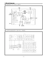
Page 66: ...66 IC Block Diagrams MAX232ECPWRP RS 232C Driver IC3801 L3E06200P0A D A S H LCD Driver IC501 IC531 IC561...

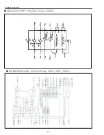
Page 67: ...67 IC Block Diagrams PW190 Scaler IC301 MR4010 Power OSC IC631...

Page 68: ...9 12 13 16 15 14 11 10 5 4 1 2 3 6 7 8 REG VCC CUT1 SEL1 FB1 IN1 REF DT1 RT OUT2 GND FB2 IN2 IN2 DT2 CS OSC Power Good Signal BIAS UVL0 BIAS 2 2V 1V lcs _ _ _ _ _ _ _ 1 5V 1 27V 2 0V ON OFF ON OFF S...

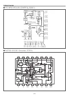
Page 69: ...69 IC Block Diagrams TB6608FNG IRIS Control IC601 TLV320AIC3105 Audio Control IC5002...

Page 70: ...MAIN BOARD A2300 R C BOARD C10 C04 S02 C12 M02 C05 S01 C03 A901 BALLAST BOARD A2200 POWER BOARD FN002 M01 LP900 Lamp Ass y S01 S01 S01 S06 S02 C08 C07 C06 A4000 AUDIO JACK BOARD SP901 Speaker SW902 L...

Page 71: ...71 Parts Location Diagrams KT8 XBM3100 Cabinet bottom 2 assembly C02 M06 FN004 C11 C01 M10 M09 M07 M05 M11 FN001 FN003 FN005 L04 Projection S04 Projection Lens...

Page 72: ...72 Parts Location Diagrams KT8 XBM3100 L07 Integrator In L08 Integrator Out L10 Integrator lens assembly S03 L09 Condenser out M04 Condenser lens Out assembly...

Page 73: ...73 Parts Location Diagrams KT8 XBM3100 S03 Ass y Condenser In Lens S03 L03 G L02 B L01 Prism LCD panel Ass y S05 S05 LCD Panel Prism Assembly...

Page 74: ...74 Parts Location Diagrams KT8 XBM3100 S03 L05 Relay out M03 Relay lens Out assembly...

Page 75: ...Optical Unit L06 L11 L03 B L03 R L02 R Marker Marker comes this side up Marker comes this side up In the optical unit CAUTION Part must be placed in specified direction when replacing the optical part...

Page 76: ...76 Parts Location Diagrams KT8 XBM3100 Accessories see accessories parts list REMOTE CONTROL MANUALs CD ROMs VGA CABLE AC CORD FILTER COVER...

Page 77: ...IS PARTS M01 610 345 0087 HOLDER LAMP BASE KR5AC M02 610 352 4184 HOLDER POWER A KR5AC M03 610 343 3721 MTG RELAY OUT KR5AC M04 610 343 3738 MTG COND OUT KR5AC M05 610 350 4469 MTG DUCT BTM IN LAMP M0...

Page 78: ...omposite STYRENE Styrene TA SOLID Tantalum Oxide Solid Electrolytic AL SOLID Aluminium Solid Electrolytic ELECT Aluminum Foil Electrolytic NP ELECT Non polarised Electrolytic OS SOLID Aluminium Solid...

Page 79: ...2SA1235A1E 305 173 9717 TR 2SA1235A1F 405 220 3115 TR ISA1235AC1E 405 220 3016 TR ISA1235AC1F Q5033 305 134 5928 TR 2SA1037AK T146 R 305 147 2218 TR 2SA1037AK S T146 305 173 9618 TR 2SA1235A1E 305 17...

Page 80: ...AMIC 15P J 50V 303 305 8515 CERAMIC 15P J 50V 404 125 8208 CERAMIC 15P J 50V C1332 403 455 5713 CERAMIC 15P J 50V 403 455 5218 CERAMIC 15P J 50V 303 305 8515 CERAMIC 15P J 50V 404 125 8208 CERAMIC 15P...

Page 81: ...76 6311 CERAMIC 0 47U K 10V C331 303 453 8917 CERAMIC 0 1U K 16V 303 453 8610 CERAMIC 0 1U K 16V 303 409 3426 CERAMIC 0 1U K 16V C332 303 453 8719 CERAMIC 470P K 50V 303 453 9211 CERAMIC 470P K 50V 30...

Page 82: ...5316 ELECT 100U M 16V 303 369 3211 ELECT 100U M 16V C3568 303 437 4614 CERAMIC 10U K 25V 403 478 5714 CERAMIC 10U K 25V C3569 303 396 9613 CERAMIC 1U K 25V 303 397 7618 CERAMIC 1U K 25V 403 478 5912...

Page 83: ...470P K 50V C413 303 453 8719 CERAMIC 470P K 50V 303 453 9211 CERAMIC 470P K 50V 303 282 5118 CERAMIC 470P K 50V C414 303 453 8917 CERAMIC 0 1U K 16V 303 453 8610 CERAMIC 0 1U K 16V 303 409 3426 CERAMI...

Page 84: ...403 455 1616 CERAMIC 10U K 16V 403 478 5813 CERAMIC 10U K 16V C507 303 358 3215 CERAMIC 10U K 6 3V 303 370 0018 CERAMIC 10U K 6 3V 303 368 7319 CERAMIC 10U K 6 3V C508 303 401 4312 ELECT 47U M 25V 303...

Page 85: ...358 3215 CERAMIC 10U K 6 3V 303 370 0018 CERAMIC 10U K 6 3V 303 368 7319 CERAMIC 10U K 6 3V C5844 403 455 1012 CERAMIC 1U K 10V 303 433 1112 CERAMIC 1U K 10V C5845 403 467 0911 CERAMIC 0 1U K 25V C586...

Page 86: ...409 3426 CERAMIC 0 1U K 16V C8817 303 453 8917 CERAMIC 0 1U K 16V 303 453 8610 CERAMIC 0 1U K 16V 303 409 3426 CERAMIC 0 1U K 16V C8818 303 453 8917 CERAMIC 0 1U K 16V 303 453 8610 CERAMIC 0 1U K 16V...

Page 87: ...390 301 224 9910 MT GLAZE 22K JA 1 16W R2395 301 298 5511 MT GLAZE 8 2K FA 1 16W R2396 301 287 2227 MT GLAZE 22K FA 1 16W R2397 301 294 3016 MT GLAZE 10K FA 1 16W R2892 301 224 8814 MT GLAZE 100 JA 1...

Page 88: ...2 7K FA 1 16W R5011 301 294 4419 MT GLAZE 1 8K FA 1 16W R5012 301 225 2019 MT GLAZE 680 JA 1 16W R5013 301 225 1418 MT GLAZE 47K JA 1 16W R5014 301 225 1418 MT GLAZE 47K JA 1 16W R5017 301 224 9316 M...

Page 89: ...13 MT GLAZE 3 3K JA 1 16W R6813 301 224 9019 MT GLAZE 10K JA 1 16W R6822 301 224 9316 MT GLAZE 1K JA 1 16W R6823 301 224 9019 MT GLAZE 10K JA 1 16W R6842 301 229 3913 MT GLAZE 180 JA 1 16W R6843 301 2...

Page 90: ...16W R9914 301 224 9019 MT GLAZE 10K JA 1 16W R9915 301 224 9019 MT GLAZE 10K JA 1 16W R9916 301 224 9019 MT GLAZE 10K JA 1 16W R9917 301 224 9019 MT GLAZE 10K JA 1 16W R9918 301 224 9019 MT GLAZE 10K...

Page 91: ...INDUCTOR 330OHM P L7811 652 002 8777 INDUCTOR 33U N L7861 645 092 8819 INDUCTOR 100U M L8801 301 037 5017 MT GLAZE 0 000 ZA 1 10W L8835 645 100 9340 IMPEDANCE 120 OHM P L8836 645 100 9340 IMPEDANCE 12...

Page 92: ...ET D SUB 15P K10B 952 001 8571 SOCKET D SUB 15P K20B 652 003 0473 JACK RCA 2 K40B 652 002 8135 PLUG D SUB 9P K9602 645 093 6760 TRANS PULSE 652 003 2743 TRANS PULSE SC2021 945 076 3503 SURGE ABSORBER...

Page 93: ...2812 L6 TB 305 015 8925 TR 2SC2812 L7 TB 305 163 1615 TR 2SC2812N L6 TB0 305 173 9816 TR 2SC3928A1R 305 173 9915 TR 2SC3928A1S Q643 305 217 6600 TR 2SK3934 Q651 305 134 5928 TR 2SA1037AK T146 R 305 14...

Page 94: ...L612 945 077 6565 INDUCTOR 900U 945 084 0273 INDUCTOR 1400U 652 003 1821 INDUCTOR 1580UH L614 910 229 3532 CORE L615 910 229 3532 CORE L616 910 229 3532 CORE L617 652 002 8500 INDUCTOR 330OHM P L631...

Page 95: ...Key No Part No Description Key No Part No Description 95 Electrical Parts List KT8 XBM3100...

Page 96: ...KT8BE November 2010 Printed in Japan 2010 Eiki Internatinal Inc A key to better communications...

Page 97: ...e manual original for chassis No KT8 XBM3100 model LC XBM31 File with the service manual No SM5111295 00 Note All the information of part numbers and values indicated on these diagrams are at the begi...

Page 98: ...al E Electrolytic P Electrolytic non polarized C Ceramic temperature compensation K Ceramic F Polyester N Polypropylene M Metalized polypropylene H Metalized polypromylar B Ceramic semiconductor G Met...

Page 99: ...1_1 25EM22005D C661 GND 1 10GJ330C R662 KK0 1LBYAG C671 GND GND 1 10GJ1KC R672 1 10GF1 2KC R676 1 10GJ3 9KC R671 25KK4 7BB C644 1 10GF3 3KC R684 RXXAV575MKBEN R614 GND 1SS355 1SS352G D613 1 10GJ10KC R...

Page 100: ...B521S 30G D1004 5VPC1 1 3GJ82 R1028 1 3GJ82 R1026 1 3GJ82 R1025 1 16GJ1 8KA R3804 1 NC 2 NC 3 NC 4 GND 5 SDA 6 SCL 7 WP 8 VDD 1 2 3 4 5 6 7 8 9 10 11 12 13 14 15 16 B4J12B13000 K20A 2 1 1 16GJ1 5KA R1...

Page 101: ...1 16GJ10KA R5840 1 16GJ10KA R5837 TXXLBB 013P Q5840 POWER_SW 1 16GJ1KA R5838 POWER_SW TPC6107P Q5830 1 2 3 4 5 6 3 3V_MCU SS3 3V SS3 3V L26B3470G L5830 3 3V_ALL 1 16GJ100KA R5822 3 3V_ALL LAMP_PWM X...

Page 102: ...2G D3623 1SS352G D3644 1SS352G D3626 1SS352G D3614 1SS352G D3613 1SS352G D3617 1SS352G D6840 1SS352G D6850 PIC_POWER_LED 1 16GJ4 7KA R6882 1SS352G D6852 1SS352G D6851 1 16GJ4 7KA R6883 1SS352G D6853 1...

Page 103: ...100 H19 101 J19 102 K19 103 L19 104 M19 105 N19 106 P19 107 R19 108 T19 109 U19 110 V19 111 W19 112 W18 113 W17 114 W16 115 W15 116 W14 117 W13 118 W12 119 W11 120 W10 121 W9 122 W8 123 W7 124 W6 125...

Page 104: ...04G TP_BENBY3 B_NRG B_DX 1 16GJ100A R513 DB_1 0 9 1 16GZ0A R503 X R502 25KK0 1MT C587 25KK0 1MT C574 25KK0 1MT C573 25KK0 1MT C579 25KK0 1MT C572 25KK0 1MT C588 25KK0 1MT C577 25KK0 1MT C576 25KK0 1MT...

Page 105: ...9909 1 16GJ100A R9908 1 16GJ100A R9907 X R9896 1 16GJ22A R9897 1 16GJ22A R9898 1 16GJ22A R9899 X R9900 1 16GJ10A R9876 1 16GJ10A R9889 1 16GJ10A R9891 1 16GJ10A R9890 X R9880 1 16GJ1 5KA R9878 1 16GJ...

Page 106: ...A10 SCH_KT8AE A8 SCH_MF4AE 1 2 3 4 5 6 7 8 9 10 11 12 13 14 15 16 A B C D E F G H I J K L A B C D E F G H I J K L NO DATA...

Page 107: ...1 PTH611H2 1LG4B10W0740A_ T6 3AH250V F601 1 2 3 4 4 3 1 2 3 4 1 2 SW602 S W 6 0 1 SW601_1 SW601_2 R614 R 635 C601 C603 C604 C606 C607 C611 C612 C613 C614 C615 LF601 C632 1 11 K6R C651 C661 C664 C665 P...

Page 108: ...RB566 R512 R513 R320 SW6801 R516 R1012 R1013 SW6803 R323 R1014 SW6804 R1016 SW6806 R3532 SW6807 SW6808 R6801 R5862 C3562 R6803 C3563 SW6810 R6804 C3564 R1215 R1021 SW6811 R5866 R6806 R1022 R1217 R6807...

Page 109: ...64 C5865 C5866 C5867 R5840 R5070 C5869 R5071 R2386 C3542 R5072 R5073 D1003 C3544 D1004 C3546 R1002 C3547 C3548 R1004 L8801 C3549 L7861 R2390 SC3801 SC3802 R2395 C3551 R2396 C3552 R2397 C3553 C3554 RB5...

Page 110: ...018 C019 C020 C021 C022 C023 C024 C025 C027 C028 C029 C030 C031 C032 C033 C034 C035 C038 C039 C041 C042 C043 C047 C048 C049 D017 D020 23 44 1 22 IC001 1 3 K8F 1 7 K002 L001 L011 L012 SC5031 SC5032 L50...

Page 111: ...K K K A K A C B E C B E C B E 1 2 3 4 5 6 Index 1 2 N Index Index 1 2 N 2 1 3 IN OUT GND 2 1 4 2 3 1 Index 1 N Index 1 N Index 1 N Index 1 N Index 1 N Index 1 N 2 1 3 1 2 3 2 1 3 GND RESET Vdd 5 3 D G...

Page 112: ...ponents or the circuit board may easily occur Because of this you should use a soldering iron and solder that satisfy the following conditions when carrying out repair work Also soldering work must be...

Reviews: