background image

EV8AQ160-DK 


36 

BDC- 1-Sep-10 


e2v semiconductors SAS 2010 


4.5.3.       

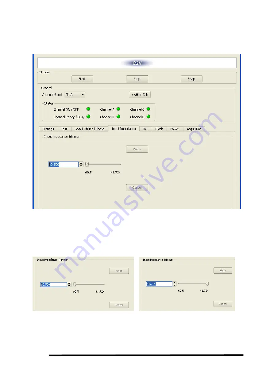
Input Impedance 


In this window, it is possible to re-adjust the internal input resistor, which should be matched to 50

The procedure is similar to the previous ones: 

-  select the channel where you need to adjust the input impedance; 

-  check that the channel is ON and READY (green LEDs); 

-  enter the resistor value; 

-  push  the WRITE  button  to  write  these  values  to  the  internal  registers  (you  can  retrieve  the 

initial value of the impedance by clicking on the CANCEL button). 


This function helps to re-adjust the input impedance in case of a slight mismatch due to temperature 

variations or process variations. 

Summary of Contents for EV8AQ160

Page 1: ...g ADC Digital outputs with an external acquisition system either with o A logic analyzer o An FPGA development board using the VITA57 FMC standard http www vita com fmc html 100 compatible with XILINX...

Page 2: ...OR STATUTORY WARRANTY RELATING TO ITS PRODUCTS INCLUDING BUT NOT LIMITED TO THE IMPLIED WARRANTY OF MERCHANTABILITY FITNESS FOR A PARTICULAR PURPOSE OR NON INFRINGEMENT IN NO EVENT SHALL E2V BE LIABLE...

Page 3: ...de where all four ADCs are all interleaved All four ADCs are clocked from the same external input clock signal and controlled via an SPI bus Serial Peripheral Interface An analog multiplexer cross poi...

Page 4: ...a PC control of ADC settings and settings for data acquisition 4 analog inputs with SMA connectors 1 clock input with SMA connector if external clock input is programming 2 SAMTEC MC HPC 8 5L connect...

Page 5: ...ted again to the ADC Demo Kit A USB driver on the ADC Demo kit allows for transmission of the data to the computer that performs the display and processing of ADC output data FFT Software and Graphica...

Page 6: ...uisition and check if sample signal is correct 13 Return to normal mode Turn OFF Test mode 14 Connect a RF generator on Analog input 15 Turn on the RF generator 16 Launch acquisition see chap Acquisit...

Page 7: ...f current is correct see chap Power Note check if test mode is OFF see chap TEST Check if acquisition mode is correctly configured Warning FFT with no windowing with no coherent signal you could have...

Page 8: ...2v semiconductors SAS 2010 With channel A and channel C with amplificatory it is needed to add RF attenuator on SMA connecter to have optimum performance Check the temperature of QUAD ADC 105 C and he...

Page 9: ...This Demo Kit board has been specially designed to be plugged with the XILINX VIRTEX 6 evaluation board EK V6 ML605 G The QUAD 8bit could be used with other FPGA evaluation boards compatible with VIT...

Page 10: ...interleaved ADC cores 1 channel mode 4 interleaved ADC cores Each channel input is driven in different ways on the board Single to Differential Amplifier from National Semiconductor A channel LMH6555...

Page 11: ...w national com ds LM LMH6555 pdf Figure 6 Channel A schematic The LMH6555 is used in DC configuration with output common mode driven by ADC QUAD 8bit This LMH6555 could be used in AC configuration Ple...

Page 12: ...ADA4939 1_4939 2 pdf Figure 8 Channel C schematic The ADA4939 1 is used in DC configuration with output common mode driven by ADC QUAD 8bit This ADA4939 1 could be used in AC configuration Please see...

Page 13: ...board via an SMA connector followed by Single to Differential Balun RF transformer MABA 007159 MACOM Please see chap 6 4 Clock selection 3 3 Control of ADC settings The Graphical User Interface allows...

Page 14: ...UI with a resolution of 2 C Please see Power In case of excessive junction temperature the ADC power supply will be turned OFF and a message will notify the user via the GUI The Demo kit provides an e...

Page 15: ...nal The QUAD 8bit requires a SYNC signal when the internal configuration is changed for example Channel configuration Dmux configuration test mode The Demo kit QUAD 8bit performs this SYNC signal auto...

Page 16: ...rom Linear Technologies Vcc 3V3 power supply with micro module LTM8023 http www linear com pc productDetail jsp navId H0 C1 C1003 C1424 P39569 Vcco and Vccd 1 8V power supply with micro module LTM8021...

Page 17: ...face software The user interface software is a Visual C compiled graphical interface that does not require a licence to run on a Windows NT and Windows 2000 98 XP PC The software uses intuitive push b...

Page 18: ...tion on your computer by launching the SetupEvalkitQuadAdc8Bits exe installer please refer to the latest version available The screen shown in Figure 5 is displayed Figure 16 demo kit QUAD 8bit applic...

Page 19: ...ep 10 e2v semiconductors SAS 2010 3 Select Components Start Menu Folder Figure 18 demo kit QUAD 8bit application Start Menu Folder 4 Select Components Additional Tasks Figure 19 demo kit QUAD 8bit app...

Page 20: ...n Ready to Install If you agree with the install configuration press Install button Now a new process of installation started Processing Display for installing Labview RunTime no license required Plea...

Page 21: ...010 6 Select Components Processing Display installation Wizard Figure 21 demo kit QUAD 8bit Processing Display installation Wizard 7 Select Components Processing Display Destination Folder Figure 22 d...

Page 22: ...8bit Processing Display Install the Application The installation of the software is now completed but you need to launch the Processing Display software This installation launch automatically 9 Selec...

Page 23: ...t application Completing Setup wizard window Figure 25 demo kit QUAD 8bit application Completing Setup wizard window Note README message Please follow instruction before using Demo kit QUAD 8bit appli...

Page 24: ...the first connection a USB driver installation will be launched Warning if you connect the Demo kit to another USB connector this installation must be re started The window shown in Figure 27 will be...

Page 25: ...5 BDC 1 Sep 10 e2v semiconductors SAS 2010 Figure 29 Browse the driver software Please choose Browse my computer for driver software advanced Figure 30 Choose the folder Select C Program Files E2V Eva...

Page 26: ...2v semiconductors SAS 2010 Figure 31 Warning installation Please choose Install the driver software anyway A Data transfer has been beginning please wait Figure 32 END of new Driver installation The n...

Page 27: ...or only if you change the USB connector you need to re install this USB driver before used After the installation you can launch the interface with the following file C Program Files E2V EvalkitQuadAd...

Page 28: ...y 1 Settings 2 Test 3 Gain Offset Phase 4 Input Impedance 5 INL 6 Clock 7 Power 8 Acquisition With Setting Test Clock and Acquisition windows always click on APPLY button to validate any command Click...

Page 29: ...ors SAS 2010 This User interface could be reduced using Hide Tab below Figure 34 User Interface Demo Kit with Hide Tab configuration This User Interface Demo show the Chip ID of QUAD 8bit at the botto...

Page 30: ...EV8AQ160 DK 30 BDC 1 Sep 10 e2v semiconductors SAS 2010 4 5 1 Setting In this window 5 functions are available ADC mode General Standby Synchronization Reset...

Page 31: ...l mode the 4 ADCs are interleaved 2 by 2 A B C D the sampling rate is equal to Fclock where Fclock is the external clock signal frequency the analogue inputs can be applied to A or B and respectively...

Page 32: ...f MSL605 evaluation board LVDS max 1GHz in speed grade 1 The capture of data QUAD 8bit at full speed must be done only in 1 2 Dmux mode The capture of data QUAD 8bit at in 1 1 Dmux mode could be done...

Page 33: ...programs the number of clock cycles prior to output clock restart after SYNC reset 4 5 2 TEST In this window the test mode is available o A ramp test is generated within each ADC and output o A flash...

Page 34: ...34 BDC 1 Sep 10 e2v semiconductors SAS 2010 Gain Offset Phase In this window you can adjust the gain offset and phase of the channel selected via the channel select button on the top right of the use...

Page 35: ...rs by clicking on the WRITE button if several adjustments are needed gain AND offset AND phase then select each value and then click on the respective WRITE buttons once all adjustments are made via t...

Page 36: ...elect the channel where you need to adjust the input impedance check that the channel is ON and READY green LEDs enter the resistor value push the WRITE button to write these values to the internal re...

Page 37: ...the INL of the ADC The process is similar to the one used for the gain offset phase adjustments select the channel where you need to adjust the INL check that the channel is ON and READY green LEDs wr...

Page 38: ...2v semiconductors SAS 2010 push the WRITE button to write these values to the internal registers push the SEND button to perform the calibration The calibration is successful if the Ext INL1 and INL1...

Page 39: ...EV8AQ160TPY DK 39 BDC 1 Sep 10 e2v semiconductors SAS 2010 INL Calibration procedure Push Load File bottom in INL calibration Select file...

Page 40: ...NL txt This file is the INL measurement of on ADC before calibration The INL measurement must be done for each channel at low analog input frequency For each channel you must create one file per ADC c...

Page 41: ...conductors SAS 2010 For this example select a channel ex A After load file the software computes automatically the INL register Note Don t forget to push write and send button After Channel A repeat t...

Page 42: ...etween the Internal PLL or external clock Note because of limitation of MSL605 evaluation board LVDS max 1GHz in speed grade 1 The capture of data QUAD 8bit at full speed must be done only in 1 2 Dmux...

Page 43: ...e2v semiconductors SAS 2010 Selection of clock PLL frequency Normal mode 2 4GHz up to 2 7GHz Divided par 2 mode 1 2 GHz up to 1 35 GHz Selection of PLL power When external clock has been chosen the cl...

Page 44: ...EV8AQ160 DK 44 BDC 1 Sep 10 e2v semiconductors SAS 2010 4 5 6 Power This sheet allows measurement of the QUAD 8bit power consumption and the internal temperature junction...

Page 45: ...EV8AQ160TPY DK 45 BDC 1 Sep 10 e2v semiconductors SAS 2010 Power when DMUX by 2 is selected Power when DMUX by 1 is selected Power when standby full is selected...

Page 46: ...EV8AQ160 DK 46 BDC 1 Sep 10 e2v semiconductors SAS 2010 4 5 7 Acquisition control This sheet controls the acquisition modes of the QUAD 8bit...

Page 47: ...d with 1024 points and INL with 4096 points Nb Harmonics Number of Harmonics takes for THD and SNR calculation Default value 10 FFT window when the analog input signal and the sampling clock are not c...

Page 48: ...e stream function Snap for single acquisition Start for continuous acquisition stop acquisition with the stop button When you launch acquisition several window results appear CH_A ADC channel A CH_B A...

Page 49: ...EV8AQ160TPY DK 49 BDC 1 Sep 10 e2v semiconductors SAS 2010 INL Curve FFT spectrum...

Page 50: ...EV8AQ160 DK 50 BDC 1 Sep 10 e2v semiconductors SAS 2010 FFT parameters Plot selection you can select one channel or several for easier reading...

Page 51: ...EV8AQ160TPY DK 51 BDC 1 Sep 10 e2v semiconductors SAS 2010 Zoom selection You can choose several kind of zoom Lock selection Cursor selection and move cursor on channel...

Page 52: ...FFT processing 02 6 5 1 log 10 10 10 log 10 02 6 5 1 log 10 1 0 0 log 10 log 20 1 1 0 1 log 10 1 1 log 10 int 1 0 1 10 10 2 1 0 dBFS dBFS THD SNR dBFS dBc dBc dBFS dBc dBc dBFS dBc dBc dBFS dB rms dB...

Page 53: ...dBc dBFS dBc dBc dBFS dBc dBc dBFS dB rms dBc rms rms dBc dBc dBc H H sig rms dB dBc SINAD ENOB SINAD SFSR SFDR SFDR SFSR SNR SNR SFSR THD THD SINAD ENOB H H Sig se AverageNoi H Sig SINAD l fundament...

Page 54: ...it configuration file It is possible to save the context of the Demo Kit saving of all settings and configuration This context can be saved for later use so that saved settings can be reloaded File DK...

Page 55: ...parameter SFDR THD SNR SINAD EBOB of each Channel A B C D in line Harmonic level of each Channel A B C D in columns FFT Module and FFT frequency of each Channel A B C D in columns File DK BDC QUAD8bi...

Page 56: ...10 e2v semiconductors SAS 2010 4 5 11 Regional and Language Options Use a control Regional Setting to check if decimal separator is configured with a dot Figure 38 Regional and Language Options Select...

Page 57: ...EV8AQ160TPY DK 57 BDC 1 Sep 10 e2v semiconductors SAS 2010 Figure 39 Customize regional Option Sheet Numbers The decimal separator must be configured with a dot...

Page 58: ...gned to be used with ML605 Xilinx Virtex 6 evaluation board Warning Please configure your LM605 evaluation board with correct Switch configuration 5 1 Software configuration XILINX configuration VIRTE...

Page 59: ...nected the USB Mini cable on USB JTAG connector J22 Change the Configuration Mode Switch and System ACE Address Lunch the iMPACT of ISE suite and load the auto_project ipf Target FPGA Virtex6 BPI Flas...

Page 60: ...p level simplify block diagram VHDL simplify SERDES diagram for each ADC output bit SERDES SERDES SERDES SERDES A AL AH ADR B BL BH BDR C CL CH CDR D DL DH DDR FIFO RAM FIFO RAM FIFO RAM FIFO RAM SPI...

Page 61: ...gurations 6 1 Channel A The Chanel A could be used in AC configuration mode by replacing R54 and R55 with a 10nF Capacitor It is possible to manipulate the output offset using R107 or R108 Inject curr...

Page 62: ...sed in AC configuration mode by replacing R51 and R84 with a 10nF Capacitor The gain of differential ADC driver could be changed by altering the values of R40 R43 R44 and R45 6 3 Channel D The Chanel...

Page 63: ...EV8AQ160TPY DK 63 BDC 1 Sep 10 e2v semiconductors SAS 2010...

Page 64: ...ock can be used for frequency different than PLL The selection between the two clocks is done manually with a resistor Remove R15 and R37 resistor and solder R36 and R50 with a 0 Note The code supplie...

Page 65: ...d by the FX2 microcontroller but this signal could also be controlled by FPGA The selection between the two clocks is done manually with a resistor Note e2v doesn t provide the SPI controller FPGA cod...

Page 66: ...e SYNC signal is control by FX2 microcontroller but this signal could be controlled by the FPGA The selection between the two clocks is done manually with a resistor Note e2v doesn t provide the SYNC...

Page 67: ...EV8AQ160TPY DK 67 BDC 1 Sep 10 e2v semiconductors SAS 2010 7 Electrical schematic Figure 40 Power supplies management...

Page 68: ...EV8AQ160 DK 68 BDC 1 Sep 10 e2v semiconductors SAS 2010 Figure 41 Temperature sense and current measurement...

Page 69: ...EV8AQ160TPY DK 69 BDC 1 Sep 10 e2v semiconductors SAS 2010 Figure 42 FX2 microcontroller and ADC level shifting...

Page 70: ...EV8AQ160 DK 70 BDC 1 Sep 10 e2v semiconductors SAS 2010 Figure 43 ADC QUAD 8bit signal configuration and decoupling capacitor...

Page 71: ...EV8AQ160TPY DK 71 BDC 1 Sep 10 e2v semiconductors SAS 2010 Figure 44 Analog input configuration and SYNC signal...

Page 72: ...EV8AQ160 DK 72 BDC 1 Sep 10 e2v semiconductors SAS 2010 Figure 45 Output connector HPC port A and Port B...

Page 73: ...EV8AQ160TPY DK 73 BDC 1 Sep 10 e2v semiconductors SAS 2010 Figure 46 Clock configuration and PLL...

Page 74: ...EV8AQ160 DK 74 BDC 1 Sep 10 e2v semiconductors SAS 2010 Figure 47 Output connector HPC port C and Port D...

Page 75: ...EV8AQ160TPY DK 75 BDC 1 Sep 10 e2v semiconductors SAS 2010 Figure 48 Level shifting VITA EEPROM Power good generation...

Page 76: ...EV8AQ160 DK 76 BDC 1 Sep 10 e2v semiconductors SAS 2010 8 Layout information Figure 49 Top side Layer 1 Figure 50 internal Layer 2...

Page 77: ...EV8AQ160TPY DK 77 BDC 1 Sep 10 e2v semiconductors SAS 2010 Figure 51 internal Layer 3 Figure 52 internal Layer 4...

Page 78: ...EV8AQ160 DK 78 BDC 1 Sep 10 e2v semiconductors SAS 2010 Figure 53 internal Layer 5 Figure 54 internal Layer 6...

Page 79: ...EV8AQ160TPY DK 79 BDC 1 Sep 10 e2v semiconductors SAS 2010 Figure 55 internal Layer 7 Figure 56 internal Layer 8...

Page 80: ...EV8AQ160 DK 80 BDC 1 Sep 10 e2v semiconductors SAS 2010 Figure 57 internal Layer 9 Figure 58 internal Layer 10...

Page 81: ...EV8AQ160TPY DK 81 BDC 1 Sep 10 e2v semiconductors SAS 2010 Figure 59 internal Layer 11 Figure 60 bottom side Layer 12...

Page 82: ...1 Sep 10 e2v semiconductors SAS 2010 9 Mechanical dimensions The Demo Kit board with Quad 8 bit ADC dimension is 139mm x 76 5mm x 8mm It is compatible with VITA57 FMC standard Figure 61 Mechanical dim...

Page 83: ...ep 10 e2v semiconductors SAS 2010 10 Ordering Information Table 1 Ordering information Part Number Package Temperature Screening Comments EV8AQ160TPY DK EBGA380 Ambient Prototype Used with XILINX VIRT...

Page 84: ...nitoring 14 3 5 ADC current consumption monitoring 15 3 6 ADC SYNC signal 15 3 7 DC DC converter 16 4 Software Tools 17 4 1 Overview 17 4 2 Configuration 17 4 3 User Interface installation 18 4 4 USB...

Reviews: