background image

8

DISASSEMBLY

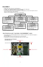
•  Disassemble in order of the arrow in the following 

fi

 gure.

•  In the case of the re-assembling, assemble it in order of the reverse of the following 

fl

 ow.

•  In the case of the re-assembling, observe "attention of assembling".
•   If wire bundles are untied or moved to perform adjustment or replace parts etc., be sure to rearrange them neatly as 

they were originally bundled or placed afterward.
Otherwise, incorrect arrangement can be a cause of noise generation.

About the photos used for "descriptions of the DISASSEMBLY" section

•   The shooting direction of each photograph used herein is indicated on the left side of the respective photograph as 

"Shooting direction: ***".

•  Refer to the diagram below about the shooting direction of each photograph.
•  Photographs with no shooting direction indicated were taken from the top of the set.

The viewpoint of each photograph
(Shooting direction)

View from the top

Front side

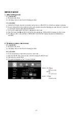
Shooting direction: B

Shooting direction: D

Shooting direction: C

Shooting direction: A

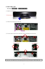
FRONT PANEL ASSY

Refer to

 "DISASSEMBLY 

1. FRONT PANEL ASSY"

and 

"EXPLODED VIEW"

KEY PWB UNIT

(Ref. No. of EXPLODED VIEW : 4)

DISPLAY PWB UNIT

(Ref. No. of EXPLODED VIEW : 6)

IR PWB UNIT

Refer to

 "DISASSEMBLY 

5. IR PWB UNIT"

and 

"EXPLODED VIEW"

IR PWB UNIT

(Ref. No. of EXPLODED VIEW : 3)

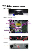
BD MAIN UNIT

Refer to

 "DISASSEMBLY 

2. BD MAIN UNIT"

and 

"EXPLODED VIEW"

MAIN PWB UNIT

(Ref. No. of EXPLODED VIEW : 1)

TOP COVER 

DC FAN

Refer to

 "DISASSEMBLY 

3. DC FAN"

and 

"EXPLODED VIEW"

DC FAN

(Ref. No. of EXPLODED VIEW : 27)

AUDIO PWB UNIT

Refer to

 "DISASSEMBLY 

6. AUDIO PWB UNIT"

and 

"EXPLODED VIEW"

AUDIO PWB

(Ref. No. of EXPLODED VIEW : 7)

POWER PWB UNIT

Refer to

 "DISASSEMBLY 

4. POWER PWB UNIT"

and 

"EXPLODED VIEW"

POWER PWB UNIT

(Ref. No. of EXPLODED VIEW : 2)

SUB POWER PWB UNIT

(Ref. No. of EXPLODED VIEW : 5)

Summary of Contents for DBP-2012UDCI

Page 1: ... 6 Some illustrations using in this service manual are slightly different from the actual set Please use this service manual with referring to the operating instructions without fail For purposes of improvement specifications and design are subject to change without notice S0532 0V06DM DG1209 Please refer to the MODIFICATION NOTICE ...

Page 2: ...ortant safety parts that are indicated by the z mark on schematic diagrams and parts lists be sure to use the designated parts Be sure to mount parts and arrange the wires as they were originally placed For safety seasons some parts use tapes tubes or other insulating materials and some parts are mounted away from the surface of printed circuit boards Care is also taken with the positions of the w...

Page 3: ...RC Composition RS Metal oxide film RW winding RN Metal film RK Metal mixture P Pulse resistant type NL Low noise type NB Non burning type FR Fuse resistor F Lead wire forming 2B 1 8 W 2E 1 4 W 2H 1 2 W 3A 1 W 3D 2 W 3F 3 W 3H 5 W F 1 G 2 J 5 K 10 M 20 Ex RN Type 14K Shape and per formance 2E Power 182 Resist ance G Allowable error FR Others Resistance 1800ohm 1 8kohm 1 8 2 Indicates number of zero...

Page 4: ...evoelig voor elektrostatische ontladingen ESD Onzorgvuldig behandelen tijdens reparatie kan de levensduur drastisch doen verminderen Zorg ervoor dat u tijdens reparatie via een polsband met weerstand verbonden bent met apparaat Houd componenten en hulpmiddelen ook op ditzelfde potentiaal Tutti IC e parecchi semi conduttori sono sensibili alle scariche statiche ESD La loro longevita potrebbe essere...

Page 5: ...perly grounded to remove any static electricity that may be charged on the body 2 Ground for Workbench Be sure to place a conductive sheet or copper plate with proper grounding 1 MΩ on the workbench or other surface where the semi conductors are to be placed Because the static electricity charge on clothing will not escape through the body grounding band be careful to avoid contacting semi conduct...

Page 6: ...S HD 3D Analog audio output Output level 2 Vrms 10 kΩ 2 channels output terminal Pin jack 1 set 7 1 channels output terminal Pin jack 1 set Audio output characteristics 1 Frequency response q BD Linear PCM 2Hz 22kHz 48kHz sampling 2Hz 44kHz 96kHz sampling 2Hz 88kHz 192kHz sampling w DVD Linear PCM 2Hz 22kHz 48kHz sampling 2Hz 44kHz 96kHz sampling 2Hz 88kHz 192kHz sampling e Super Audio CD 2Hz 40kH...

Page 7: ...LX 108 z Refer to MEASURING METHOD AND WAVEFORMS When you repair the BD MECHA UNIT you can use the following JIG Please order it from Denon Official Service Distributor in your region if necessary Do not supply it 2 Dimensional Bar Code Reader DS6708 made by Symbol Co etc 1 Set Do not supply it 232C TTL USB conversion jig Model DUT 06635 by GeeeTech 1 Set Part No 61205000300AS 4P RE PH CONN CORD 1...

Page 8: ...hooting direction indicated were taken from the top of the set The viewpoint of each photograph Shooting direction View from the top Front side Shooting direction B Shooting direction D Shooting direction C Shooting direction A FRONT PANEL ASSY Refer to DISASSEMBLY 1 FRONT PANEL ASSY and EXPLODED VIEW KEY PWB UNIT Ref No of EXPLODED VIEW 4 DISPLAY PWB UNIT Ref No of EXPLODED VIEW 6 IR PWB UNIT Ref...

Page 9: ... the claw and move in the direction of arrow to gradually pull out the assembly Proceeding TOP COVER FRONT PANEL ASSY Shooting direction B J4 FFC cable Shooting direction D View from the bottom Shooting direction C Please refer to EXPLODED VIEW for the disassembly method of each P W B included in FRONT PANEL ASSY ...

Page 10: ...he connector wires and FFC cables 3 Remove the screws 4 Remove the screw Proceeding TOP COVER REAR PANEL ASSY BD MAIN UNIT Shooting direction B BACK PANEL ASSY BD MAIN UNIT CN5 FFC cable FFC cable FFC cable N2 FFC cable JP2 Shooting direction A View from the bottom ...

Page 11: ...NIT Proceeding TOP COVER DC FAN Please refer to EXPLODED VIEW for the disassembly method of CD FAN Proceeding TOP COVER CD FAN POWER PWB UNIT Please refer to EXPLODED VIEW for the disassembly method of POWER PWB UNIT Proceeding TOP COVER IR PWB UNIT Please refer to EXPLODED VIEW for the disassembly method of IR PWB UNIT Proceeding TOP COVER AUDIO PWB UNIT Please refer to EXPLODED VIEW for the disa...

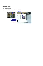
Page 12: ...12 REMOVING DISCS 1 Remove the Top Cover 2 Open the CD tray by turning the Drive gear counterclockwise Shooting direction D Drive gear ...

Page 13: ...AGNOSTICS OF OPTICAL PICKUP d M q 1 M w M M M M M M 1 Laser drive current initial value 1 1 1 11 1 1 T 2 1 m m m m n n n n 1 1 1 11 1 1 T 2 2 m m m m n n n n 1 1 1 11 1 1 T 2 3 m m m m n n n n M M 1 q M M w ...

Page 14: ... m m m m n n n n X 1 CD laser mode 2 DVD laser mode 3 BD SL laser mode mmmm mA Initial value nnnn mA Current value 2 To clear the accumulated laser on time Press the 1 button while the accumulated laser on time is displayed TC1 TC2 TC3 until TC4 clear appears at the display If the 1 button is pressed the accumulated laser on time of CD DVD and BD is cleared FL Display The display part of 13 digits...

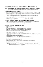
Page 15: ...DBP2012 see DISASSEMBLY 2 Follow the firmware update procedure and update the firmware to the latest version see VERSION UPGRADE PROCEDURE OF FIRMWARE 2 How to Replace the BD MECHA UNIT ASSY 2 1 Devices Used 1 PC 2 2 Dimensional Bar Code Reader DS6708 made by Symbol Co etc Do not supply 3 USB 232C TTL conversion jig Model DUT 06635 by GeeeTech Do not supply 4 4P RE PH CONN CORD 1000mm Part No 6120...

Page 16: ... of the set before the BD MECHA UNIT ASSY is replaced 2 Decompress the D M ScanBarcode Rpower 2 16 60 KES460 _ MP function zip folder and start the Rpower exe 3 A pop up is displayed Click OK 4 Click OK to PC USB MAIN PWB UNIT CN601 4P RE PH CONN CORD 1000mm Jumper pin 3 3V f mark USB 232C TTL conversion jig View from the bottom 2 Dimensional Bar Code BD MECHA UNIT ASSY for replacement The 2 dimen...

Page 17: ...17 5 On the screen below select ComPort XX Select the USB 232C TTL conversion jig port 6 Check Directory ...

Page 18: ...d reading the barcode the read data is displayed b If the 2 dimensional barcode data has already been read by the 2 dimensional barcode reader and the converted data obtained copy the data from the data file and paste it into this section NOTE Be sure not to mistake the light pick up bar code data settings with data from a different pick up Writing incorrect data will cause laser degradation Click...

Page 19: ...hen Pass changes to green writing to the Flash ROM of the MAIN PWB UNIT is complete 11 Switch off the set unit power and remove the 232C TTL side 4P PH connector of the USB 232C TTL conversion jig from the MAIN PWB UNIT CN601 ...

Page 20: ...unit see DISASSEMBLY 2 Remove the MECHA COVER 3 Cut wire clamp band then disconnect the connector wire and FFC cable 4 Move the optical pickup to the outer circumference remove the FFC Cable and remove the screws MECHA COVER HA700 FFC cable MAIN PWB UNIT cut FFC cable OPTICAL PICKUP ...

Page 21: ...on off mode in the test mode page 25 Check that the values are 6 mA from the initial value for BD and 12 mA from the initial value for DVD CD 2 Clear the total laser usage time see the procedure for clearing the accumulated laser on time in test mode page 26 3 Check BD DVD and CD media playback 4 If there are no problems with playback remove the disc press the ON STANDBY button to switch to standb...

Page 22: ...IZING is displayed on the FL tube 3 The display on the FL tube switches to INITIALIZED the NO DISC display reappears and initialization is completed 2 Firmware version check mode 2 1 preparation 1 Equipment used None 2 Unit setting No spec other than the following procedure 2 2 procedure b Front end and Back end and SYS com version check mode 1 Press the SETUP button on the remote controller to di...

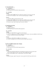
Page 23: ...procedure 4 2 procedure Setting 1 Pressing the PURE DIRECT and 3 buttons for simultaneously 2 Lock On is displayed on the FL tube and operations with the remote control and the REMOTE CONTROL input terminal on the back of the DBP 2012UD are disabled Cancel 1 Pressing the PURE DIRECT and 3 buttons for simultaneously 2 Lock Off is displayed on the FL tube and remote lock mode is made canceled 5 All ...

Page 24: ... page 15 b When choose OPU change mode and press the 1 button press the 2 button and please cancel a mode 6 Test mode cancel TI q When the 9 button is pressed after entering the test mode the display switches in the order T2 T7 TC TG TI T2 FL Display The display part of 13 digits 1 2 3 4 5 6 7 8 9 10 11 12 13 T 2 L a s e r O n O f f FL Display The display part of 13 digits 1 2 3 4 5 6 7 8 9 10 11 ...

Page 25: ...ss the 1 button to begin error rate measurement The address and error rate are displayed For a description of the displayed measurement results see Table 1 Error rate details FL Display The display part of 13 digits 1 2 3 4 5 6 7 8 9 10 11 12 13 T Y Y m m m m m m l l l l YY selection mode 71 to 94 m address PBA HEX l error rate COUNT SEC DEC Note CD 4x speed Renewal of data is carried out for ever...

Page 26: ...me of CD DVD and BD is cleared FL Display The display part of 13 digits 1 2 3 4 5 6 7 8 9 10 11 12 13 T C 1 0 h When TC1 TC2 or TC3 is selected with the 8 or 9 button mmmmmm is displayed as 0 so you can check 4 Picking up No display mode Press the 8 or 9 button to switch to the pickup number display The pickup number is a 15 digit number so it is displayed in two sections FL Display The display pa...

Page 27: ...erence of 1 layer It is invalid It is invalid C2 uncorrectable error number When this is selected for BD or DVD T74 FFFFFFFFFF display 75 The central circumference of 1 layer BIS error detection signed number It is invalid It is invalid When this is selected for DVD or CD T75 FFFFFFFFFF display 76 The central circumference of 1 layer It is invalid It is invalid It is invalid When this is selected ...

Page 28: ...umber It is invalid When this is selected for DVD 1 layer or CD T89 FFFFFFFFFF display 90 The central circumference of 2 layer It is invalid It is invalid It is invalid When this is selected for BD DVD or CD T90 FFFFFFFFFF display 91 The outer circumference of 1 layer BIS error detection signed number It is invalid It is invalid When this is selected for DVD or CD T91 FFFFFFFFFF display 92 The out...

Page 29: ...s to select Update then press the ENTER button During update the power indicator lights in red and the GUI screen disappears And an approximately remaining time is indicated on the display When updating is complete the power indicator lights in green and normal status is resumed 5 Press the SETUP button to close the menu Cautions on Firmware Update In order to update the firmware you must have the...

Page 30: ...Normally 3 3V is output OK if 3 3V is output even momentarily Check parts surrounding and soldering N105 15PIN FFC 1 0mm MAIN UNIT U16 CS8966F PQFP447 and other circuits Check AC_DET signal output N105 1 AC50Hz 50Hz 1 2Vp p AC60Hz 60Hz 1 2Vp p Check parts surrounding and soldering D112 D113 IN4007 U105 PC817 and other circuits Defect of primary circuit component D101 RBV1506 U102 STR W6753 U103 ST...

Page 31: ...ring U3 MR 6625UYB J1 20x1 W HOUSING POWER UNIT T101 AEP ERL28075 SW_TRANS D115 FS34 N101 20P FMN and other circuits Check parts surrounding and soldering U5 PT6302 J1 20x1 W HOUSING POWER UNIT T101 AEP ERL28075 SW_TRANS D118 FR107 N101 20P FMN and other circuits NO NO NO YES YES Check parts surrounding and soldering U5 PT6302 U3 MR 6625UYB J1 20x1 W HOUSING POWER UNIT N101 20P FMN N105 15P FMN MA...

Page 32: ...nal to U20 Is data input to 6pin Are 3 3V supplied to 1pin Check soldering U20 U100 U20 1pin and 6pin and surrounding circuitry END NO YES Check output terminal Is data output from the VIDEO OUT terminal of J861 Check soldering J816 and surrounding circuitry NO NO NO YES YES YES Check output signal from U20 Is data output from 27pin Check soldering U20 U20 27pin and surrounding circuitry ...

Page 33: ...ut Is the signal output to DOCMP_Y7_R12 Y0_N16 DOCMP_Cb7_T4 Cb0_T12 and DOCMP_Cr7_ M15 Cr0_J16 Are 3 3V supplied to DDST_RSTn_M9 Check output signal of U228 Is the signal output from 44pin 43pin and 42pin Check output signal of U20 Is the signal output from 23pin 21pin and 18pin Are 3 3V supplied to 15pin Check the voltage of the output terminal Is data output from the COMPONENT VIDEO OUT terminal...

Page 34: ...ave of 27MHz output to X6 Are 3 3V supplied to RST_2015_N Check output signal of U225 Is the signal of DOHM_CLK_A10 VS_A15 HS_B13 DE_A13 output Is the signal output to DOHM_Y11_C7 Y0_C12 DOHM_Cb11_A9 Cb0_B12 and DOHM_Cr11_C3 Cr0_B6 Are 3 3V supplied to DDST_RSTn_M9 Check output signal U25 Is the signal output from 30pin 31pin 33pin 34pin 36pin 37pin 39pin and 40pin Are 3 3V supplied to 30pin Check...

Page 35: ...61 Check the digital signal for 3Vpp Replace the MAIN UNIT Replace C868 R868 R866 Q211 R862 R864 R863 R869 3 5 Ether is not connection Check the input signal of U901 SMSC8710 Check the power supply voltage Replace the MAIN UNIT Check the POWER UNIT NO YES Check the output signal of U901 SMSC8710 Replace the MAIN UNIT NO Check soldering D23 P900 YES NO NO YES YES ...

Page 36: ...ding circuitry Check data signal to Each DAC U1 DAC for MIX 2ch L R 4 5 6 7pin IIS format 4pin LRCK fs rate 5pin DATA 6pin BCK 64 fs rate 7pin SCK MCK rated 256 384 512 fs Same applies to other channel U101 FL FR U111 C SW U201 SL SR U211 SBL SBR Check soldering MUTE and surrounding circuitry MUTE Transistors Q2 5 Q8 11 for MIX ch Q2 Q5 Base voltage is about 8 8V during playback Q101 104 for FL FR...

Page 37: ...ent Title 1 chapter 1 Color Bar 100 Main Menu 59 94Hz 1080i 1 Video signal 1 Color Bar 100 Component output resolution 1080i It is better to use wires for extending between the probe and test points Since there are no test points for locations q to r confirm the signals at the land of a chip resistor MAIN UNIT TEST POINT AND WAVEFORMS A Component side Detail A 4 3 2 1 5 GND ...

Page 38: ...38 qU20 NJM2566 _Video out_signal C32 w rU20 NJM2566 _Component out_Y Cb Cr signal Y C29 Cb C30 Cr C31 Video out_signal q Component out_Y signal w Component out_Cb signal e Component out_Cr signal r ...

Page 39: ...39 Terminal output check Video Out terminal check Component Out terminal check DBP 2012 Oscilloscope 75ohm Load Video out_signal Component out_Y signal Component out_Cb signal Component out_Cr signal ...

Page 40: ...40 Personal notes ...

Page 41: ...ransceiver SMSC8710 㪜㪫㪟㪜㪩㪥㪜㪫 㪉㪌㪤 POWER PWB 㪝㪝㪚㩷㪉㪇㪧 SMPS 12V 㪧㪟㩷㪈㪊㪧 Standby SMPS Sub Power 㫋㫆㩷㪤㪘㪠㪥㩷㪧㪮㪙 㫋㫆㩷㪛㪠㪪㪧㪣㪘㪰㩷㪧㪮㪙 㪝㪝㪚㩷㪐㪧 㪝㪝㪚㩷㪈㪌㪧 㪽㫉㫆㫄㩷㪤㪘㪠㪥㩷㪧㪮㪙 㪝㪝㪚㩷㪈㪌㪧 㫋㫆㩷㪧㪦㪮㪜㪩㩷㪧㪮㪙 㪧㪟㩷㪈㪊㪧 㪽㫉㫆㫄㩷㪧㪦㪮㪜㪩㩷㪧㪮㪙 㪩㪼㪾㫌㫃㪸㫋㫆㫉 㪧㪟㩷㪌㪧 FAN IR PWB 㪝㪝㪚㩷㪐㪧 㪮㪠㪩㪜㪛㩷㪩㪜㪤㪦㪫㪜 DISPLAY PWB FL TUBE IR MODULE FL DRIVE BUTTON SW KEY PWB B to B BUTTON SW LED 㪝㪝㪚㩷㪉㪇㪧 㪽㫉㫆㫄㩷㪧㪦㪮㪜㪩㩷㪧㪮㪙 㪧㪟㩷㪌㪧 㪬㪪㪙 㪉㪎㪤 㪧㪟㩷㪉㪧 I P Scaler ABT2015BG316 㪛㪛㪩㪉 㪲㪢㪋㪫㪌㪈㪈㪍㪊㪨㪞㪴 㪛...

Page 42: ...IR UNIT FAN AUDIO UNIT 5P PH PH 5P PH 9P FFC P1 0 45P FFC P0 5 HA700 J700 HA600 JT10 J2 N301 16P B to B J4 J405 J407 N105 N104 15P FFC P1 0 13P PH PH N102 N103 N101 K101 AC INLET 20P FFC P1 0 JP1 JP2 9P B to B 14P B to B CN5 J306 JV101 12P FFC P1 0 2P PH HA701 N1 HA1 N2 J1 WIRING DIAGRAM ...

Page 43: ...43 8 7 6 5 4 3 2 1 M L K J I H G F E D C B A PRINTED WIRING BOARDS MAIN COMPONENT SIDE 鉛フリー半田 半田付けには 鉛フリー半田 Sn Ag Cu を使用してください Lead free Solder When soldering use the Lead free Solder Sn Ag Cu ...

Page 44: ...44 1 2 3 4 5 6 7 8 M L K J I H G F E D C B A MAIN FOIL SIDE 鉛フリー半田 半田付けには 鉛フリー半田 Sn Ag Cu を使用してください Lead free Solder When soldering use the Lead free Solder Sn Ag Cu ...

Page 45: ... 12 5 D126 T102 12 5 D127 12 5 D129 12 5 D130 JV35 7 5 JV36 7 5 C101 C127 R148 D131 R149 D123 Q104 Q105 Z101 R107 L106 D124 J101 JV45 JV15 JV27 JV28 JV29 JV39 7 5 JV50 7 5 JV51 7 5 JV52 7 5 JV53 7 5 JV54 7 5 JV19 7 5 JV38 JV40 JV42 JV43 JV44 JV47 JV55 JV56 JV57 JV58 JV59 JV64 JV65 JV3 JV10 JV13 JV20 JV25 JV34 12 5 JV41 12 5 JV61 12 5 JV5 12 5 JV6 12 5 JV8 12 5 JV11 12 5 JV14 12 5 JV16 12 5 JV18 12...

Page 46: ...143 R144 R145 R146 R147 C111 C113 C114 C115 C116 C123 C128 C130 C132 C133 C134 C135 C136 C137 C138 C139 C140 C143 C145 C146 C147 C149 C150 C152 C153 C154 C156 C157 C158 C159 C160 C161 C162 C163 C164 C165 C166 C167 C168 C169 C170 C171 C172 D125 D128 D120 D121 R150 R151 C173 1 2 3 4 5 6 7 8 9 10 11 12 13 G F E D C B A 鉛フリー半田 半田付けには 鉛フリー半田 Sn Ag Cu を使用してください Lead free Solder When soldering use the Le...

Page 47: ... C156 R46 C157 R47 C158 R48 C163 C164 C165 C166 R59 R60 Z1 Z2 Z3 Z4 Z6 C1 C45 C46 C53 C54 C57 C56 C24 R210 C25 R211 C26 R212 C27 R213 C28 R214 C29 R215 R216 R217 R218 R219 C30 C31 R220 R221 U101 R222 U102 R223 U103 R224 U104 R225 U111 R232 U112 R233 U113 R234 U114 C49 R235 R236 R237 R238 C50 C51 C52 R241 C205 R242 C206 R243 C207 R244 C208 R245 C209 R246 R247 R248 R249 C210 C211 C212 R250 Q10 R251 ...

Page 48: ...213 C214 C215 C216 C217 C218 C219 C220 C221 C227 C228 C229 D201 D202 D203 Q201 Q202 Q204 L201 L202 L203 L204 L205 R201 R202 R203 R204 R206 R207 R208 R209 Q205 R225 R228 R227 R226 1 2 3 4 5 6 D C B A 1 2 3 4 5 6 7 C B A 1 2 3 4 C B A BD 100109 01 SUB POWER BOARD 1 2 3 4 5 6 7 8 9 10 11 12 G F E D C B A 鉛フリー半田 半田付けには 鉛フリー半田 Sn Ag Cu を使用してください Lead free Solder When soldering use the Lead free Solder ...

Page 49: ... R118 OPEN Z101 SCK10054MSY AEP ERL28075 SW_TRANS T101 2 3 4 6 8 9 10 11 12 13 14 15 16 U101 1 2 PHOTO_COUPLER EL817 U101 2 2 U104 2 2 U104 PHOTO_COUPLER EL817 1 2 U107 PHOTO_COUPLER EL817 1 2 U107 2 2 U106 1 2 U106 PHOTO_COUPLER EL817 1 2 U105 PHOTO_COUPLER EL817 2M 3216 R102 2M3216 R101 2M3216 R104 2M 3216 R103 C107 1000P 250V Y1 C104 0 22 250V X2 C106 470P 250V Y1 C105 470P 250V Y1 C103 470P 25...

Page 50: ...P_MINI JACK HSJ1003 016020 K203 GND 1 2 2 3 3 GND 21 2 22 3 23 S201 OPEN 1 2 3 4 5 L205 BLM21PG121SN1D 2125 L204 BLM21PG121SN1D 2125 L203 BLM21PG121SN1D 2125 L201 BLM21PG121SN1D 2125 L202 BLM21PG121SN1D 2125 C224 0 1 50 GR C223 0 1 50 GR C225 0 1 50 GR C209 220P 1608 C205 0 1Z1608 C206 1000P 1608 GND2 S303 GND2 D301 SMLU12416W S 1 RED 2 3 GRN N301 16P PLUG_FH708V P2 54mm_FEMALE_SIDE 1 2 3 4 5 6 7 ...

Page 51: ... N1 1 2 3 4 5 6 7 8 9 14P TUCP SOCKET N2 1 2 3 4 5 6 7 8 9 10 11 12 13 14 4 7u C11 4 7u C12 4 7u C31 4 7u C32 22u C6 22u C16 22u C17 22u C26 22u C36 22u C37 BLM18PG330SN1D 1608 L1 BLM18PG330SN1D 1608 L2 BLM18PG330SN1D 1608 L4 BLM18PG330SN1D 1608 L5 BLM18PG330SN1D 1608 L6 BLM18PG330SN1D 1608 L7 BLM18PG330SN1D 1608 L9 BLM18PG330SN1D 1608 L10 91K R8 91K R17 6 2M R19 6 2M R20 OPEN C9 OPEN C18 OPEN C19...

Page 52: ... GR9 40 GR8 39 GR7 38 GR6 37 GR5 36 GR4 35 GR3 34 GR2 33 GR1 32 SG35 31 SG34 30 SG33 29 SG32 28 SG31 27 SG30 26 SG29 25 GR14 45 GR15 46 GR16 47 VEE 48 VSS 49 OSCI 50 OSCO 51 RSTB 52 CSB 53 CLKB 54 DIN 55 VDD 56 P1 57 P2 58 AD2 59 AD1 60 SG1 61 SG2 62 SG3 63 SG4 64 U5 PT6302 U5 PT6302 D3 NC D3 NC R25 39k 1 R25 39k 1 D4 NC D4 NC R13 10k NC R13 10k NC D1 NC D1 NC D2 NC D2 NC D7 BAT85 D7 BAT85 LED1 DU...

Page 53: ...N2 27P FFC 1 2 3 4 5 6 7 8 9 10 11 12 13 14 15 16 17 18 19 20 21 22 23 24 25 26 27 R6 22 R2 22 R8 22 DGND R3 22 N1 1 2 3 4 5 NJM4565M U4 7 8 6 5 BA15218F U2 7 4 6 5 BA15218F U2 1 8 2 3 BA15218F U3 1 8 2 3 BA15218F U3 7 4 6 5 D2 1SS301 1 2 3 D1 1SS301 1 2 3 D5 1SS301 1 2 3 D4 1SS301 1 2 3 TC74LCX125FT EL U7 1 1G 2 1A 3 1Y 4 2G 5 2A 6 2Y 7 GND 8 3Y 9 3A 10 3G 11 4Y 12 4A 13 4G 14 VCC TC74LCX157FT EL...

Page 54: ...JM4565M U102 1 8 2 3 AGND C122 0 018 PCM1795_PIN6_BCK2 C118 100 16 RA3 R128 2 2K C116 1000P R167 100 C129 100 50 RFO R148 270 AGND NJM4565M U102 7 4 6 5 R182 OPEN AGND U111 PCM1795DBR 1 ZEROL 28 Vcc2L 27 AGND3L 26 IoutL 25 IoutL 24 AGND2 23 Vcc1 22 VcomL 21 VcomR 20 Iref 19 AGND1 18 IoutR 17 IoutR 16 AGND3R 15 Vcc2R 2 ZEROR 3 MSEL 4 LRCK 5 DATA 6 BCK 7 SCK 8 DGND 9 VDD 10 MS 11 MDI 12 MC 13 MDO 14...

Page 55: ...0K C254 2200P NJM4565M U212 7 4 6 5 D204 1SS301 1 2 3 AGND DGND C221 6800P AGND TPF61 R277 10K NJM4565M U202 1 8 2 3 C226 2200P R271 2 2K R217 820 R227 47K R203 33 AGND C216 1000P Q216 DTC114EK AGND R261 390 DGND C230 100 16 RA3 R202 33 TPF64 AGND Q214 DTA114EK AGND R269 2 2K R214 75 R263 47K C205 0 1 R235 2 2K C255 2200P C261 0 1 R210 270 C238 0 1 AGND 9V AGND MCU_SCL R239 10 C252 0 018 AGND R247...

Page 56: ...1 R384 100 R384 100 C479 100pF NC C479 100pF NC C481 C481 100pF NC 1V1TP SMD D1 0 1V1 C35 NC C35 NC R49 10 R49 10 CE27 220uF 10v CE27 220uF 10v B_KEY_IN B_KEY_IN VCC TP SMD D1 0 VCC TP SMD D1 0 D S G Q4 QM3001S D S G Q4 QM3001S 8 4 3 7 5 6 1 2 R47 47K R47 47K RESET TP SMD D1 0 RESET TP SMD D1 0 NC2 NC2 R50 10K R50 10K C56 1000pF C56 1000pF C559 100pF NC C559 100pF NC FB11 BLM15P FB11 BLM15P FB20 B...

Page 57: ...4 0 1uF 16V C142 0 1uF 16V C116 0 1uF 16V C116 0 1uF 16V U100A MT8530_DDR2 MT8530 BGA702 P0 695 B0 5 U100A MT8530_DDR2 MT8530 BGA702 P0 695 B0 5 VCC2IO AY14 VCC2IO BB14 VCC2IO AY30 VCC2IO BB30 VCC2IO AR31 VCC2IO AY34 VCC2IO BB34 VCC2IO W35 VCC2IO AL35 VCC2IO AY38 VCC2IO BB38 VCC2IO P40 VCC2IO V40 VCC2IO AB40 VCC2IO AF40 VCC2IO AK40 VCC2IO AP40 VCC2IO AV40 VCC2IO P42 VCC2IO V42 VCC2IO AB42 VCC2IO A...

Page 58: ... 0 1uF 16V C205 0 1uF 16V C217 0 1uF 16V C217 0 1uF 16V C238 0 1uF 50V C0603 SMD C238 0 1uF 50V C0603 SMD C224 0 1uF 16V C224 RN202 100x4 RN202 100x4 C236 0 1uF 16V C236 0 1uF 16V R200 0 R200 0 C202 0 1uF 16V C202 0 1uF 16V C226 0 1uF 16V C226 R206 100 R0603 SMD R206 100 R0603 SMD TP200 TP200 C212 0 1uF 16V C212 0 1uF 16V C227 0 1uF 16V C227 C219 0 1uF 16V C219 0 1uF 16V C230 0 1uF 16V C230 0 1uF ...

Page 59: ...z Y201 27 0000MHz C934 0 1uF C934 0 1uF R950 560_1 R950 560_1 FB202 BLM15P FB202 BLM15P FB205 BLM15P FB205 BLM15P TP213 TP213 C948 22pF C948 22pF R217 1M R217 1M TP212 TP212 R947 1M R947 1M R210 4 7k R210 4 7k U100C MT8530_DDR2 U100C MT8530_DDR2 AVDD33_VDACR AVSS33_VDACR AVDD33_VDACY AVSS33_VDACY AVDD33_VDACBG AVSS33_VDACBG AVDD33_XTAL AVSS33_XTAL AVDD33_XTAL25M AVSS33_XTAL25M AVDD33_SACD AVSS33_S...

Page 60: ...R R1243 0R TP306 TP306 TTRST TTRST U301 M25P16 NC CASON8 SMD U301 M25P16 NC CASON8 SMD S_ 1 Q 2 W_ VPP 3 VSS 4 D 5 C 6 HOLD_ 7 VCC 8 GND13 GND13 TP303 TP303 C309 0 1uF C309 0 1uF R307 4 7K R307 4 7K R1182 10K R1182 10K R322 0 R322 0 RN300 22x4 RN300 22x4 1 2 3 4 5 6 7 8 TTCK TTCK R302 10K R302 10K R310 10K NC R310 10K NC FB302 BLM15P FB302 BLM15P FB307 BLM15P FB307 BLM15P C308 NC C308 NC FB308 BLM...

Page 61: ...pping Pin Boot ICE 0402 For STBY MCU 232 VFD IR RS232 0402 VCC3IO_STB Below 20mA AVDD33_LDO Below 20mA CNT MII HW TRAPPING D3V3 D3V3 R421 NC R421 NC R414 10K R414 10K C402 0 1uF NC C402 0 1uF NC R416 10K R416 10K U100D MT8530_DDR2 MT8530 BGA702 P0 695 B0 5 U100D MT8530_DDR2 MT8530 BGA702 P0 695 B0 5 VCC3IO_STB J33 VCC3IO_STB G35 AVDD33_LDO J37 AVSS33_LDO K36 AVDD10_LDO H38 ETCOL C37 ETCRS H34 ETMD...

Page 62: ...LK1 12 VOUTCLK2 12 VOUT0 12 VOUT1 12 VOUT2 12 VOUT3 12 VOUT4 12 VOUT5 12 VOUT6 12 VOUT7 12 VOUT8 12 VOUT9 12 VOUT10 12 VOUT11 12 VOUT12 12 VOUT13 12 VOUT14 12 VOUT15 12 VOUT16 12 VOUT17 12 VOUT18 12 VOUT19 12 SPDIF_HDMI 16 AO2MCLK 16 AO2SDATA4 16 AO2SDATA5 16 DOES_OEn_D15 15 DORS_OEn_D16 15 CCIR_IN_Y9 19 SiI9134_WS 16 SiI9134_SCLK 16 SiI9134_SD0 16 SiI9134_SD1 16 SiI9134_SD2 16 SiI9134_SD3 16 ASPD...

Page 63: ...33 39K R633 39K TP734 TP734 R650 NC R650 NC R606 0 NC R606 0 NC C622 0 1uF C622 0 1uF C610 0 1uF C610 0 1uF NC611 NC611 C650 0 1uF C650 0 1uF C996 0 1uF C996 0 1uF CE706 100uF 16V CE706 100uF 16V V612 V612 C600 0 1uF NC C600 0 1uF NC MPX2 MPX2 TP760 TP760 TP614 TP614 R630 3K R630 3K C641 2 2uF 6 3v C641 2 2uF 6 3v TP745 TP745 C608 0 1uF C608 0 1uF R1028 0 R1028 0 NO600 NO600 C1004 0 1uF C1004 0 1u...

Page 64: ...R1035 0 C1019 NC C1019 NC C1026 NC C1026 NC C1023 NC C1023 NC R705 10K R705 10K V14REF V14REF U700 R2A30209SP SSOP42 SMD U700 R2A30209SP SSOP42 SMD SPIN 1 SL1IN 2 SL2IN 3 SPLIN 4 VM2 5 SL2 6 GND 7 SL2 8 SL1 9 SL1 10 GND 11 U 12 V 13 W 14 ACTFLG 15 COMMON 16 TEST 17 SLLIM 18 FG 19 EN1 20 EN2 21 REF 42 LOIN 41 FOIN 40 TOIN 39 TLIN 38 TL 37 TL 36 FO 35 FO 34 GND 33 5VCC 32 TO 31 TO 30 GND 29 LO 28 LO...

Page 65: ...RST MIX_MCU_SDA MIX_MCU_SDA R658 0 R658 0 AOSDATA4 AOSDATA4 FB37 BLM15P FB37 BLM15P FB29 BLM15P FB29 BLM15P AOLRCK AOLRCK AOMCLK AOMCLK HA1 AUDIO_CON IMSA 9610S 27Y919 HA1 AUDIO_CON IMSA 9610S 27Y919 1 2 3 4 5 6 7 8 9 10 11 12 13 14 15 16 17 18 19 20 21 22 23 24 25 26 27 GND9 GND9 R394 33 R394 33 R562 100 R562 100 R374 100 R374 100 FB34 BLM15P FB34 BLM15P R725 33 R725 33 AMUTE AMUTE C1029 100pF NC...

Page 66: ... C987 33PF R985 33 R985 33 R999 0 R999 0 R1006 10K R1006 10K D23 RClamp0524S D23 RClamp0524S 1 1 2 2 3 3 4 4 5 5 6 6 C976 0 1uF C976 0 1uF C988 33PF C988 33PF R1017 10K NC R1017 10K NC R983 1 5K R983 1 5K R929 49 9 R929 49 9 C985 0 1uF C985 0 1uF R168 0 R168 0 R995 0 R995 0 C977 0 1uF C977 0 1uF R991 75 R991 75 R987 47 R987 47 C3 22PF NC C3 22PF NC R931 10 R931 10 GND6 GND6 R986 47 R986 47 U901 SM...

Page 67: ...TO_VS_N2 15 ABTO_Y2_K1 15 ABTO_Y0_G1 15 ABTO_Y1_B3 15 ABTO_CbCr2_M2 15 ABTO_CbCr0_R1 15 ABTO_CbCr1_P2 15 ABTO_Y5_K3 15 ABTO_Y3_J2 15 ABTO_Y4_J3 15 ABTO_CbCr5_M3 15 ABTO_CbCr3_M4 15 ABTO_CbCr4_L4 15 ABTO_Y8_H1 15 ABTO_Y6_J1 15 ABTO_Y7_H3 15 ABTO_CbCr8_M8 15 ABTO_CbCr6_M1 15 ABTO_CbCr7_L2 15 ABTO_Y9_G3 15 ABTO_Y10_H2 15 ABTO_CbCr11_K2 15 ABTO_CbCr9_L1 15 ABTO_CbCr10_L3 15 ABTO_HS_N1 15 ABTO_CLK_H5 1...

Page 68: ...R436 33R DQ11 DQ11 R425 33R R425 33R R280 33R R280 33R C325 0 1uF 16v C325 0 1uF 16v R327 33R R327 33R R444 33R R444 33R CE32 100uF 10v LESR CE32 100uF 10v LESR C330 0 1uF 16v C330 0 1uF 16v C335 0 1uF 16v C335 0 1uF 16v C346 0 1uF 16v C346 FB35 BLM21P FB35 BLM21P 3V3 3V3 C344 0 1uF 16v C344 C349 0 1uF 16v C349 0 1uF 16v C354 22uF 6 3V C354 U17 uP7706U8 U17 uP7706U8 POK 1 EN 2 VIN 3 CNTL 4 NC 5 VO...

Page 69: ...H32M16BN 25E A0 M8 A1 M3 A2 M7 A3 N2 A4 N8 A5 N3 A6 N7 A7 P2 A8 P8 A9 P3 A10 M2 A11 P7 A12 R2 ODT K9 CK J8 CK K8 CKE K2 CS L8 RAS K7 CAS L7 WE K3 BA0 L2 BA1 L3 LDM F3 UDM B3 UDQS B7 UDQS A8 LDQS F7 LDQS E8 DQ0 G8 DQ1 G2 DQ2 H7 DQ3 H3 DQ4 H1 DQ5 H9 DQ6 F1 DQ7 F9 DQ8 C8 DQ9 C2 DQ10 D7 DQ11 D3 DQ12 D1 DQ13 D9 DQ14 B1 DQ15 B9 VDD A1 VDD E1 VDD M9 VDD J9 VDD R1 VDDL J1 VDDQ A9 VDDQ C1 VDDQ C3 VDDQ C7 V...

Page 70: ...C7 16 1HTR6_C6 16 1HTR9_C9 16 1HTR8_C8 16 1HTR11_C11 16 1HTR10_C10 16 ABTO_CLK_H5 12 DOES_OEn_D15 7 DORS_OEn_D16 7 TO SiI9134 FROM ABT2015 TO VIDEO ENCODER FOR COMPON Connect the DOES_OEn_D15 and DORS_OEn_D16 to MT8530 IC FB49 BLM15P FB49 BLM15P R164 100 R164 100 R79 22 R79 22 DV_TDATA_S DV_TDATA_S R82 22 R82 22 R77 22 R77 22 C84 0 1uF 50V C84 0 1uF 50V R152 NC R152 NC C78 0 1uF 50V C78 0 1uF 50V ...

Page 71: ...2 72 D23 71 D24 70 D25 69 D26 68 D27 67 D28 63 D29 62 D30 61 D31 60 D32 59 D33 58 D34 57 D35 56 DE 1 HSYNC 2 VSYNC 3 IDCK 88 SPDIF 4 MCLK 5 SCK 11 WS 10 SD0 9 SD1 8 SD2 7 SD3 6 EXT_SWG 27 TX0 33 TX0 34 TX1 36 TX1 37 TX2 39 TX2 40 TXC 31 TXC 30 DSCL 46 DSDA 47 DDCPWR5V 45 HPD 51 INT 24 CSCL 48 CSDA 49 CI2CA 50 TMODE 52 DCLK 15 DR0 16 DL0 17 DL1 19 DR1 18 DL2 21 DR2 20 DL3 23 DR3 22 C458 C458 0 1uF ...

Page 72: ...220uF 16v R721 NC R721 NC R517 0 C522 NC C522 NC R473 22 R473 22 C503 10uF 50V C503 10uF 50V C92 0 1uF 50V C92 0 1uF 50V R472 NC R472 NC R467 33 R467 33 R643 0 R643 0 L72 NC L72 NC L75 NC L75 NC Q12 2SA1022 Q12 2SA1022 1 3 2 R503 330 R503 330 R480 33 R480 33 R483 0 R483 0 R464 510 1 R464 510 1 R520 NC R520 NC C438 1000pF C438 1000pF L81 10uH L81 10uH L74 NC L74 NC R549 4 7K R549 4 7K R476 1 5K R47...

Page 73: ...877 NC C877 NC C551 10uF NC C551 10uF NC R714 75_1 R714 75_1 R670 47K R670 47K R868 68 R868 68 U26 TC7S08F U26 TC7S08F 1 2 3 5 4 C32 470uF 6 3v C32 470uF 6 3v CB9 0 1uF 16V CB9 0 1uF 16V R653 0 R653 0 R718 NC R718 NC C540 0 1uF 50V C540 0 1uF 50V C182 NC C182 NC R740 0 R740 0 R567 NC R567 NC R867 0 R867 0 CB8 0 1uF 16V CB8 0 1uF 16V R869 100K R869 100K R565 75_1 R565 75_1 C189 NC C189 NC P6 COAX P...

Page 74: ...7K R291 4 7K R666 10K R666 10K Q213 NC Q213 NC TOP J306 CON12 1 0 TOP J306 CON12 1 0 C170 0 1uF 16V C170 0 1uF 16V 5V_RS232 5V_RS232 CN5 2PIN1 25 NC CN5 1 2 CEC CEC R271 33 R271 33 R137 NC R137 NC R342 33 D19 1SS355 D19 1SS355 R128 18K R128 18K R290 10K R290 10K MCU_3V3 MCU_3V3 R668 NC R668 NC R282 33 R282 33 R65 1 24K_1 R65 1 24K_1 R256 100 R256 100 R71 0 R71 0 R735 10K R735 10K R258 33 R258 33 R...

Page 75: ... 27 28 12 16 2 26 5 41 1 17 18 106 x14 101 x4 x4 x4 103 x2 104 x5 101 x4 104 x4 107 x4 103 x5 101 x4 101 x3 101 201 202 x6 103 x1 105 103 x8 x3 106 x1 102 x2 104 x4 a Parts marked with this symbol have critical characteristics Use ONLY replacement parts recommended by the manufacturer WARNING 印の部分は安全を維持するために重要 な部品です 従って交換時は必ず指定の 部品を使用してください 75 ...

Page 76: ...Personal notes Personal notes 76 ...

Page 77: ...0S BD MAIN UNIT DBP2012 7025HV1004010 1 1 nsp MAIN PWB UNIT ASSY 1 11 963309100060S BD MECHA UNIT ASSY DBP2012 8038041679010S 1 11a 45301003200AS CLAMPER ASS Y for BD MECHA F 9332H DZ11 182 1 67 nsp 9P FFC 1 0 N711091033810S 1 12 nsp MECHA BRACKET 4010215106100S 1 13 nsp DAMPER 60X10 4050213415000S 1 14 nsp DAMPER 40X35 4050213425000S 1 15 nsp DAMPER 75X35 4050213435000S 1 17 nsp HEAT SHEET 25X25 ...

Page 78: ...000S 1 37 nsp OPEN CLOSE KNOB 1611SP SP 5090214591100S 1 38 nsp KNOB 1P 1611BK BK 5097214611000S 1 38 nsp KNOB 1P 1611SP SP 5097214611100S 1 39 nsp WINDOW 1611 5077213133000S 1 52 nsp BUFFER 10x150x10t 1 40 nsp EMIGASKET NLCG100100 15mm 4400210619000S 1 41 nsp ALUMINUM TAPE 35mm 1220210978000S 1 42 418510021006D LOADER PANEL 1611BK BK 4317215341000S 1 42 418510021013D LOADER PANEL 1611SP SP 431721...

Page 79: ...972652000210S FUSE 3 15AH 250V G650202255510S 1 z K101 972641000080S AC INLET AC M34U E3 G430341535510S 1 z K101 972641000510S AC INLET AC M34 E2 E1 G430040600020S 1 z T101 972102000220S SW_TRANS 8200380285020S 1 IR PWB UNIT Ref No 3 K201 00D2051305008 232C Terminal L103090090030S 1 K203 00D2048729008 MINI 2P Jack IR INOUT G401HSJI05500S 1 KEY PWB UNIT Ref No 4 N301 645010079000S 16P PLUG P 2 54mm...

Page 80: ...80 PACKING VIEWs 7 8 8 14 15 16 17 19 18 17 16 19 9 13 12 11 10 z 1 3 4 5 6 ...

Page 81: ...3002S 1 6 nsp ADDENDUM SHEET UPDATE_YOUTUBE 5227000001880S 1 7 nsp CABINET COVER 6327040022012S 1 8 972532000470D CUSHION 2012 L R 6230213024000S 1 9 nsp POLY COVER 6337040062010S 1 z 10 972611000410S AC CORD 2000mm UL 7A 125V E3 L068125075550S 1 z 10 972611000420S AC CORD 1500mm CB 2 5A 250V E2 E1 L068250250440S 1 11 nsp YAF11 0745N 3PIN RCA VIDEO L R 1 5M L063152030020S 1 12 nsp BATTERY SUM 3 AS...

Page 82: ... P3 4 Not use Hi Z Hi Z Not use 11 P4 3 MCU_SCL O High 3 3V Hi Z 4 7K PU I2C Clock signal is for EEPRM IC 24C02 12 VSS Power Ground Voltage 13 RXVDD Power VDD for RTC 14 RXIN Not use I Crystal IN for RTC oscillator 15 RXOUT Not use O Crystal OUT for RTC oscillator 16 P4 2 MCU_SET3 I High 3 3V or Low 0V High 3 3V or Low 0V 10k PU MCU setting pin by externail resistance Default is high 17 P1 7 MCU_A...

Page 83: ...y I High 3 3V High 3 3V 10k PU Power key signal input terminal Fall edge is valid 33 VSS Power Not use 34 VDD2 5 Power Internal Regulator Output 2 5V 35 VDD Power Supply Voltage 3 3V 36 RSTN RSTN I High2 5V Low 0V Reset Low active 37 P2 4 Not use Hi Z Hi Z Not use 38 P2 5 Not use Hi Z Hi Z Not use 39 P2 6 Not use Hi Z Hi Z Not use 40 P2 7 CEC_RS232_SWITCH O Low 0V High 3 3V 10k PU Switch singal is...

Page 84: ...p t u o r o t a l l i c s O O O C S O RSTB I Reset input pin When this pin is set to LOW all functions are initialized 52 CSB I Chip select input pin When this pin is set to High Level the serial data transfer is disabled 53 CLKB I Shift clock input pin The serial data is shifted at the rising edge of CLKB 54 5 5 n i p t u p n i a t a d l a i r e S I N I D 6 5 y l p p u s r e w o p e v i t i s o P...

Page 85: ...85 MT8530 MAIN UNIT U100 Block Diagram MT8530 OPU Motor Driver FLASH DRAM Audio DAC HDMI CVBS Component Ethernet USB 2 0 ...

Page 86: ...86 LAN8710 MAIN UNIT U901 Block Diagram ...

Page 87: ...87 NJM2566AV MAIN UNIT U20 Block Diagram ...

Page 88: ... AGND1 IOUTRï IOUTR AGND3R VCC2R Power Supply RST SCK Advanced Segment DAC Modulator IOUTL IOUTLï IOUTRï Current Segment DAC IOUTR Bias and Vref VCOML VCOMR AGND2 V DD V CC 1 V CC 2L V CC 2R AGND1 I V and Filter 8 Oversampling Digital Filter and Function Control Audio Data Input I F LRCK BCK DATA MDO MDI MC MS AGND3L AGND3R DGND Current Segment DAC IREF VOUTL I V and Filter VOUTR Function Control ...

Page 89: ...input 1 MDI 11 I Mode control data input 1 MDO 13 I O Mode control readback data output 3 MS 10 I O Mode control chip select input 2 MSEL 3 I I2C SPI select 1 RST 14 I Reset 1 SCK 7 I System clock input 1 VCC1 23 ï Analog power supply 5 V VCC2L 28 ï Analog power supply L channel DACFF 5 V VCC2R 15 ï Analog power supply R channel DACFF 5 V VCOML 22 ï L channel internal bias decoupling pin VCOMR 21 ...

Page 90: ...2 C2 R2IN T2OUT VCC T1OUT R1IN R1OUT T1IN T2IN R2OUT GND V VCC 5V 2 V 16 T1OUT T2OUT T1IN T2IN T1 T2 11 10 14 7 5V 400kΩ 5V 400kΩ R1OUT R1IN R1 13 12 5kΩ R2OUT R2IN R2 8 9 5kΩ 10V TO 10V VOLTAGE INVERTER 0 1μF 6 V C2 C2 0 1μF 4 5 5V TO 10V VOLTAGE INVERTER C1 C1 0 1μF 1 3 0 1μF GND 15 ...

Page 91: ...91 2 FL DISPLAY FL TUBE 15 BT 114GNK Display UNIT U3 ...

Page 92: ...92 Personal notes ...

Reviews: