


7.Electrical Interface
© China Daheng Group, Inc. Beijing Image Vision Technology Branch 25
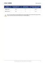
Parameter
Test condition
Value (us)
Rising edge delay
VIN=5V
3.02
~
6.96
VIN=12V
2.46
~
5.14
Falling edge delay
VIN=5V
6.12
~
17.71
VIN=12V
8.93
~
19.73
Table 7-4 Delay time of opto-isolated input circuit in typical application environment
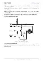
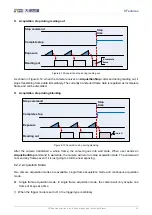
TRIGIN_F_DELAY
TRIGIN_R_DELAY
2V
0.8V
LINE0+
INPUT0
Figure 7-4 Parameter of opto-isolated input circuit
Rising time delay (TRIGIN_R_DELAY): the time required for the response to the decrease to 0.8V of
INPUT0 from 50% rising of LINE0+
Falling time delay (TRIGIN_F_DELAY): the time required for the response to the rise to 2V of INPUT0
from 50% falling of LINE0+
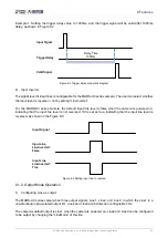
7.3.2. Line1 (Opto-isolated Output) Circuit
Hardware schematics of opto-isolated output circuit is shown as Figure 7-5.
9
1
2
3
4
5
6
7
8
12
11
10
Rexternal
EXVCC
Line1+
Line1-
OUTPUT1
External circuit
Figure 7-5 Opto-isolated output circuit
Range of external voltage (EXVCC) is 5~24V
Maximum output current of Line1 is 25mA


