


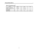


25
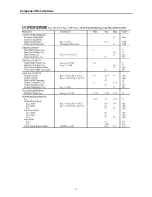
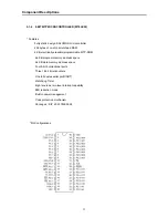
* Features
• Low-Voltage and Standard-Voltage Operation
– 5.0 (V CC = 4.5V to 5.5V)
– 2.7 (V CC = 2.7V to 5.5V)
– 2.5 (V CC = 2.5V to 5.5V)
– 1.8 (V CC = 1.8V to 5.5V)
• Internally Organized 128 x 8 (1K), 256 x 8 (2K), 512 x 8 (4K),1024 x 8 (8K) or 2048 x 8 (16K)
• 2-Wire Serial Interface
• Schmitt Trigger, Filtered Inputs for Noise Suppression
• Bidirectional Data Transfer Protocol
• 100 kHz (1.8V, 2.5V, 2.7V) and 400 kHz (5V) Compatibility
• Write Protect Pin for Hardware Data Protection
• 8-Byte Page (1K, 2K), 16-Byte Page (4K, 8K, 16K) Write Modes
• Partial Page Writes Are Allowed
• Self-Timed Write Cycle (10 ms max)
• High Reliability
– Endurance: 1 Million Write Cycles
– Data Retention: 100 Years
– ESD Protection: >3000V
• Automotive Grade and Extended Temperature Devices Available
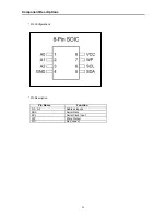
• 8-Pin and 14-Pin JEDEC SOIC, 8-Pin PDIP, 8-Pin MSOP, and 8-Pin TSSOP Packages
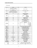
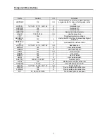
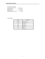
Component Descriptions
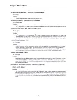
2-1-7 Serial EEPROM, 2K (256 x 8) (AT24C02)
Summary of Contents for DVC-T6300N
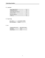
Page 10: ...10 2 1 3 NTSC PAL Digital Video Encoder AD7170 Component Descriptions ...
Page 11: ...11 Component Descriptions ...
Page 12: ...12 Component Descriptions ...
Page 14: ...14 Functional Description Component Descriptions ...
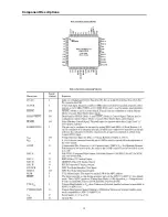
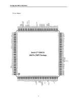
Page 15: ...15 Component Descriptions Pinout Diagram ...
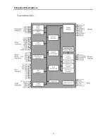
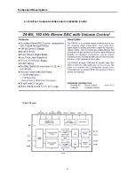
Page 18: ...18 Block Diagram Component Descriptions 2 1 5 DIGITAL TO ANALOG STEREO AUDIO CONVERTER CS4391 ...
Page 19: ...19 Component Descriptions ...
Page 20: ...20 Component Descriptions ...
Page 21: ...21 Component Descriptions ...
Page 28: ...28 Component Descriptions ...
Page 30: ...30 Component Descriptions ...
Page 31: ...31 Component Descriptions ...
Page 54: ...54 9 PCB Diagrams 9 1 Main PCB Top ...
Page 55: ...55 PCB Diagrams 9 2 Main PCB Bottom ...
Page 56: ...56 9 3 Front PCB Top 9 4 Front PCB Bottom PCB Diagrams ...
Page 57: ...57 9 5 SMPS PCB Top 9 6 SMPS PCB Bottom PCB Diagrams ...
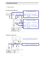
Page 58: ...58 10 Wiring Diagram ...
Page 65: ...65 11 3 SMPS PCB Schematic Diagram 11 3 SMPS PCB Schematic diagram ...
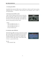
Page 66: ...66 1 27MHz 2 ROM DATA BUS 3 RAM DATA BUS 4 12C CLK 5 12C DATA 6 HSYNC 12 Oscillograms ...
Page 67: ...67 7 VSYNC 8 BCLK DVD 9 LRCK DVD 10 TSDO 11 MCLK 12 HOST DATA Oscillograms ...
Page 68: ...68 13 HOST CLK 14 HOST CS 15 MC DACO 16 MD DACO 17 VFD DATA 18 VFD STB Oscillograms ...
Page 70: ...70 MEMO ...


