


16
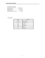
*Pin Description
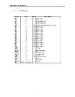
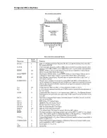
Name
Number
I/O
Definition
VCC
1, 9, 18, 27, 35, 44, 51, 59, 68, 75,
83, 92, 99, 104, 111,
121, 130,
139, 148, 157, 164, 172, 183,
193, 201
I
3.65 V ± 150 mv.
LA[21:0]
23:19,16:10,7:2,207:204
O
Device address output.
VSS
8,17,26,34,43,52,60,67,76,84,91
,98,103112,120,129,138,147,15
6,163,171,177,184,192,200,208
I
Ground.
RESET#
24
I
Reset input, active low.
TDMDX
O
TDM transmit data
RSEL
25
I
ROM Select
RSEL Selection
0
16-bit ROM
1 8-bit ROM
TDMDR
28
I
TDM receive data.
TDMCLK
29
I
TDM clock input.
TDMFS
30
I
TDM frame synch.
TDMTSC#
31
O
TDM output enable, active low.
TWS
SEL_PLL1
32
O
I
Audio transmit frame sync.
Select PLL1.
TSD
SEL_PLL0
33
O
I
Audio transmit serial data port.
Select PLL0.
SEL_PLL2 SEL_PLL0 Clock Output
0 0 2.5 x DCLK
0 1 3 x DCLK
1 0 3.5 x DCLK
1 1 4 x DCLK
SEL_PLL2
36
Select PLL2. See the table for pin number 33.
MCLK
39
I/O
Audio master clock for audio DAC.
TBCK
40
I/O
Audio transmit bit clock.
SDIF_DOBM
41
O
S/PDIF (IEC958)Format Output.
RSD
45
I
Audio receive serial data.
RWS
46
I
Audio receive frame synch.
RBCK
47
I
Audio receive bit clock.
APLLCAP
48
I
Analog PLL Capacitor.
XIN
49
I
Crystal input.
XOUT
50
O
Crystal output.
DMA[11:0]
66:61, 58:53
O
DRAM address bus.
DCAS#
69
O
Column address strobe, active low.
DOE#
DSCK_EN
70
O
I
Output enable, active low.
Clock enable, active low.
DWE#
71
O
DRAM write enable, active low.
DRAS[2:0]#
74:72
O
Row address strobe, active low.
DB[15:0]
96:93, 90:85, 82:77
I/O
DRAM data bus.
DCS[1:0]#
97, 100
O
SDRAM chip select [1:0], active low.
DQM
101
O
Data input / output mask.
DSCK
102
O
Clock to SDRAM.
DCLK
105
I
Clock Input(27MHz).
YUV[7:0]
115:113, 110:106
O
8-bit YUV output.
PCLK2XSCN
116
I/O
2X pixel clock.
PCLKQSCN
117
I/O
Pixel clock.
1. VSY
NC
H#
118
I/O
Vertical synch for screen video interface,
programmable for rising or falling edge, active
low.
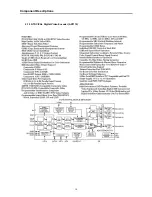
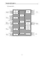
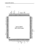
Component Descriptions
Summary of Contents for DVC-T6300N
Page 10: ...10 2 1 3 NTSC PAL Digital Video Encoder AD7170 Component Descriptions ...
Page 11: ...11 Component Descriptions ...
Page 12: ...12 Component Descriptions ...
Page 14: ...14 Functional Description Component Descriptions ...
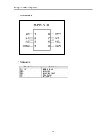
Page 15: ...15 Component Descriptions Pinout Diagram ...
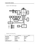
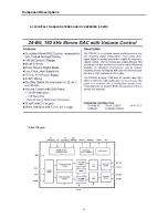
Page 18: ...18 Block Diagram Component Descriptions 2 1 5 DIGITAL TO ANALOG STEREO AUDIO CONVERTER CS4391 ...
Page 19: ...19 Component Descriptions ...
Page 20: ...20 Component Descriptions ...
Page 21: ...21 Component Descriptions ...
Page 28: ...28 Component Descriptions ...
Page 30: ...30 Component Descriptions ...
Page 31: ...31 Component Descriptions ...
Page 54: ...54 9 PCB Diagrams 9 1 Main PCB Top ...
Page 55: ...55 PCB Diagrams 9 2 Main PCB Bottom ...
Page 56: ...56 9 3 Front PCB Top 9 4 Front PCB Bottom PCB Diagrams ...
Page 57: ...57 9 5 SMPS PCB Top 9 6 SMPS PCB Bottom PCB Diagrams ...
Page 58: ...58 10 Wiring Diagram ...
Page 65: ...65 11 3 SMPS PCB Schematic Diagram 11 3 SMPS PCB Schematic diagram ...
Page 66: ...66 1 27MHz 2 ROM DATA BUS 3 RAM DATA BUS 4 12C CLK 5 12C DATA 6 HSYNC 12 Oscillograms ...
Page 67: ...67 7 VSYNC 8 BCLK DVD 9 LRCK DVD 10 TSDO 11 MCLK 12 HOST DATA Oscillograms ...
Page 68: ...68 13 HOST CLK 14 HOST CS 15 MC DACO 16 MD DACO 17 VFD DATA 18 VFD STB Oscillograms ...
Page 70: ...70 MEMO ...