3. PB MODE
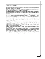
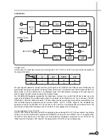
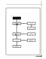
(1) Signal Flow
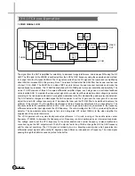
FM signal input to the Pin 13rd is amplified, and ditributed to the two BPFs-1.4MHz and 1.8MHz. The band passed
FM signals are supplied to the De-Modulator unit. First, the FM LIM confines the FM to the limitted level, and then the
signals are demodulated. The converted audio signals are compensated by the SW NOISE COMPEN. The signals
are passed by the LPF, and de-emphasized by the FM DE-EMPH in order to restrict the FM back-noise. The PNR
processor expands the signals and reduces the audio noise.
The two Line AMPs amplifiy the audio level, and supply to the Audio Out Pin 30th, 29th. The Mod out Pin 27th is and
mixed audio output port for the RF-modulator. The Output SW is available to select the audio output of Left+Right
(Stereo), Left only, Right only and Normal Audio. The Pin 26th is the input port for Normal audio.
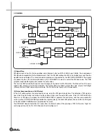
(2) Noise Compensation and Hi-Fi Detect
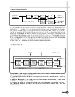
In the Hi-Fi audio system, the noise trouble occurs, when the FM signal is defective. The defection of FM signal is
due to the Drop Out which is scratched on the surface of tape, and the audio SW noise. If the D.O. DET detects the
Drop Out of FM signal, it requires the HOLD PULSE GEN to generate the hold pulse, and then compensate the
noise. And the HOLD PULSE GEN generates the regular pulse by the Audio SW pulses, then send the control signal
to the SW NOISE COMPEN which compensates the noise.
The ENVE/HiFi discreminates the Hi-Fi audio from the Normal audio. If the envelope of FM Hi-Fi exists, “High”-5V-
control signal is out to the Pin 14th. Otherwise Control voltage is 0.
18
CIRCUIT
FM PB IN
13
Hi-Fi DET
14
AUDIO OUT(L)
MOD OUT
30
AUDIO OUT(R)
29
26
8
AMP
LPF
LPF
FM
LIM
DEMOD
D.O.
DET
HOLD
PULSE GEN
SW NOISE
COMPEN.
PNR
OUTPUT
SW
LPF
FM
DE-EMPH
FM
DE-EMPH
FM
LIM
DEMOD
FM
DET
SW NOISE
COMPEN.
FM
ALC
ENVE/
HiFi
A SW
PULSE
PNR
27
AMP
AMP
NORMAL AUDIO
LPF
Summary of Contents for DV-K88 series
Page 71: ...68 CIRCUIT DIAGRAMS 9 1 Connection Diagram SECTION 9 CIRCUIT DIAGRAM 68...
Page 72: ...69 CIRCUIT DIAGRAMS R819 5 1 9 2 Power Circuit Diagram...
Page 73: ...70 CIRCUIT DIAGRAMS 9 3 Syscon and Logic Circuit Diagram...
Page 74: ...71 CIRCUIT DIAGRAMS 9 4 AV SW Circuit Diagram...
Page 75: ...72 CIRCUIT DIAGRAMS 9 5 IF PDC Circuit Diagram TM...
Page 76: ...73 CIRCUIT DIAGRAMS 9 6 If Module Circuit Diagram A2...
Page 77: ...74 CIRCUIT DIAGRAMS 9 7 If Module Circuit Diagram Nicam...
Page 78: ...75 CIRCUIT DIAGRAMS 9 8 Hi Fi Pre Amp Circuit Diagram...
Page 79: ...76 CIRCUIT DIAGRAMS 9 9 Video Audio Circuit Diagram...
Page 80: ...77 CIRCUIT DIAGRAMS 9 10 Remocon Circuit Diagram...
Page 81: ...SECTION 10 COMPONENTS LOCATION GUIDE ON PCB BOTTOM VIEW 78 P C B LOCATION 10 1 PCB Main...
Page 82: ...80 P C B LOCATION 10 3 PCB Logic DV K8K S S Series DV K86 S S Series DV K82 S S Series...
Page 83: ...81 P C B LOCATION DV K88 S S Series...
Page 84: ...SECTION 11 DISASSEMBLY 83 DISASSEMBLY 11 1 Packing Ass y...
Page 85: ...84 DIAGRAMS DV K88 Series DV K82 Series DV K8K Series DV K86 Series 11 2 Front Panel Assembly...

