4
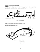
NOTE: PLACING THE UNIT IN THE SERVICE MODE
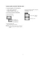
Service option
For this chassis, the sensors (start/end/reel) are located on the MAIN circuit board, not in the DECK assembly. There is an important
service option that has to be followed to repair the MAIN circuit board with the DECK assembly connected. To imitate the function of
the sensors, insert the SVC Mode Diode (D707) on the MAIN circuit board as shown below.
STOP/EJECT CH DN
POWER
CH UP
D707
REC
REW
FWD
PLAY/PAUSE
MAIN P.C.B (TOP SIDE)
PATH FIXTURE CONNECTION/TEST POINT IDENTIFICATION
Refer to the adjustment of the tape transporting system.
Connect to PT01,
!
pin-
^
pin of the
MAIN CIRCUIT BOARD.
CTL pulse test point
GND
S/W pulse test point
ENVE pulse test point
!
^
Summary of Contents for DV- K584N-SJ
Page 35: ...34 AC001 K584NZ SJ M K584NZ SG M only...
Page 36: ...35...
Page 37: ...36...
Page 38: ...37...
Page 39: ...38...
Page 60: ...59 ELECTRICAL ADJUSTMENTS Fig 1 Circuit Board Location...
Page 92: ...91 INTERCONNECT WIRING DIAGRAM K584N K484N K384N K284N...
Page 93: ...92 POWER SUPPLY SCHEMATIC DIAGRAM FREE VOLTAGE K584NY SJ M K584NZ SJ M K584NZ SG M...
Page 95: ...94 2HD HEAD AMP SCHEMATIC DIAGRAM K384N K284N K304N...
Page 96: ...95 4HD HEAD AMP SCHEMATIC DIAGRAM K584N K484N K504N...
Page 97: ...96 VIDEO AUDIO SCHEMATIC DIAGRAM K584N K484N K384N K284N K504N K304N...
Page 98: ...97 PIF INPUT SELECTOR SCHEMATIC DIAGRAM 9V USE K584NY SJ M K584NZ SJ M K584NZ SG M...
Page 100: ...99 TIMER SYSCON SCHEMATIC DIAGRAM K584N K484N K384N K284N K504N K304N...
Page 101: ...100 POWER SUPPLY BLOCK DIAGRAM FREE VOLTAGE K584NY SJ M K584NZ SJ M K584NZ SG M...
Page 103: ...102 2HD HEAD AMP BLOCK DIAGRAM K384N K284N K304N...
Page 104: ...103 4HD HEAD AMP BLOCK DIAGRAM K584N K484N K504N...
Page 105: ...104 VIDEO AUDIO BLOCK DIAGRAM K584N K484N K384N K284N K504N K304N...
Page 106: ...105 PIF INPUT SELECTOR BLOCK DIAGRAM K584N K484N K384N K284N K504N K304N...
Page 109: ...108 MAIN PCB 2HEAD 4HEAD...


