

47
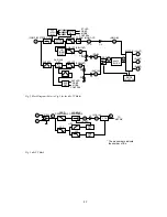
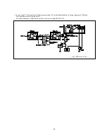
6) Operation
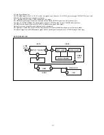
When the RF signal received by antenna is input to TMI Antenna Input and user selects a channel, the CH control data (clock, data,
enable) memorized in a MI-COM is output. The data runs PLL IC of TMI tuner part and outputs the selected channel to IF module. The
input signal in IF module is demodulated to video signal on video detector part through IF amp and saw filter, and is output through
4.5MHz trap circuit. The demodulated signal is input in FM detector circuit through 4.5MHz BPF circuit, and is demodulated to audio
signal on FM detector circuit, and is finally output. During the above process, AFT voltage is input in a MI-COM which detects AFT
(–) in 1.875V or less, or AFT (+) in 2.812V or more and the best point of the tuning is got.
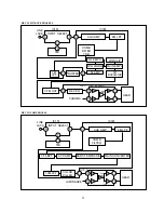
In case of Hi-Fi model, video signal out of TMI, is input to pin 3 of SW IC, where as video signal from input jack is input to pin 6. In
both cases, signal is selected by tuner/line selection signal input to pin 4. Every signal selected by SW IC, is output to pin 8 and then
input to video part.
Audio signal out of TMI is input pin 12 of MPX module (SBX1837) through variable registor for stereo separation adjustment. MPX
module makes stereo and sap signal separatedly and then they one input to MATRIX circuit through demodulation circuit MATRIX circuit
controls L out (pin 3) or R out (pin 4) by stereo/sap control signal input to pin 9,10 of MPX module, and makes them input to audio part.
In case of mono model, video signal output of TMI is input to Pin 12 of SW IC, where as video signal from input jack is input to Pin 1 of
SW IC, and Audio signal output of TMI is input to Pin 5 of SW IC, where as audio signal from input jack is input to Pin 3 of SW IC.
In both case, video & audio signal is selected by tuner/line selection signal that input to Pin 9, 10, 11.
Video signal selected by SW IC is output to Pin 14 and then input to video part. Audio signal selected by SW IC is output to Pin 4 and then
input to audio part.
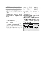
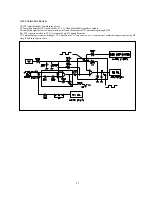
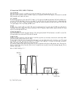
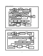
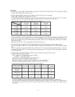
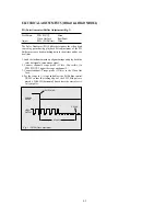
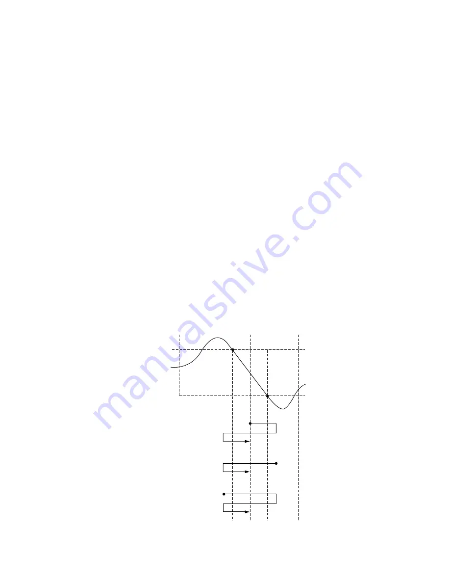
7) The operation of AFT
Sync search checks whether there is sync or not, and the search starts at center frequency. Tuning frequency is increased by 0.5MHz up
to +2MHz and decreased by 0.5MHz upto -2MHz from center frequency. If sync is detected within this range, fo ±2MHz, window
search at a detected point starts. If not, the first fo data is output as it is. AFT window search decreases/increases PLL data by 62.5 KHz
upto maximum ±2MHz (32 steps).
i) The first data is within AFT window
ii) The first data is under AFT window
iii) The first data is over AFT window
Refer to "NEXT PAGE DIAGRAM"
Sync search should be carried out in advance in order to get AFT voltage. If a channel is selected by user, channel data memorized in a
MI-COM are output to PLL IC. The PLL IC sends the fvco (local oscillation frequency) of the equivalent channel to tuner IC, and the
MI-COM check whether there is sync or not 150ms after the data output. If the sync is "low", window search is worked, and if it is
"high", sync search is done.
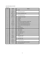
fo –2M
(AFT+)
2.81V
(AFT–)
1.88V
iii)
AFT+
fo
fo +2M
i)
ii)
i)
ii)
iii)
fo"
fo'
AFT–
Summary of Contents for DV- K584N-SJ
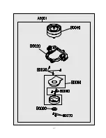
Page 35: ...34 AC001 K584NZ SJ M K584NZ SG M only...
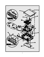
Page 36: ...35...
Page 37: ...36...
Page 38: ...37...
Page 39: ...38...
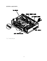
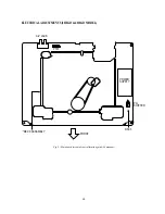
Page 60: ...59 ELECTRICAL ADJUSTMENTS Fig 1 Circuit Board Location...
Page 92: ...91 INTERCONNECT WIRING DIAGRAM K584N K484N K384N K284N...
Page 93: ...92 POWER SUPPLY SCHEMATIC DIAGRAM FREE VOLTAGE K584NY SJ M K584NZ SJ M K584NZ SG M...
Page 95: ...94 2HD HEAD AMP SCHEMATIC DIAGRAM K384N K284N K304N...
Page 96: ...95 4HD HEAD AMP SCHEMATIC DIAGRAM K584N K484N K504N...
Page 97: ...96 VIDEO AUDIO SCHEMATIC DIAGRAM K584N K484N K384N K284N K504N K304N...
Page 98: ...97 PIF INPUT SELECTOR SCHEMATIC DIAGRAM 9V USE K584NY SJ M K584NZ SJ M K584NZ SG M...
Page 100: ...99 TIMER SYSCON SCHEMATIC DIAGRAM K584N K484N K384N K284N K504N K304N...
Page 101: ...100 POWER SUPPLY BLOCK DIAGRAM FREE VOLTAGE K584NY SJ M K584NZ SJ M K584NZ SG M...
Page 103: ...102 2HD HEAD AMP BLOCK DIAGRAM K384N K284N K304N...
Page 104: ...103 4HD HEAD AMP BLOCK DIAGRAM K584N K484N K504N...
Page 105: ...104 VIDEO AUDIO BLOCK DIAGRAM K584N K484N K384N K284N K504N K304N...
Page 106: ...105 PIF INPUT SELECTOR BLOCK DIAGRAM K584N K484N K384N K284N K504N K304N...
Page 109: ...108 MAIN PCB 2HEAD 4HEAD...


