background image

FM33256B

Document Number: 001-86213 Rev. *C 

Page 17 of 39

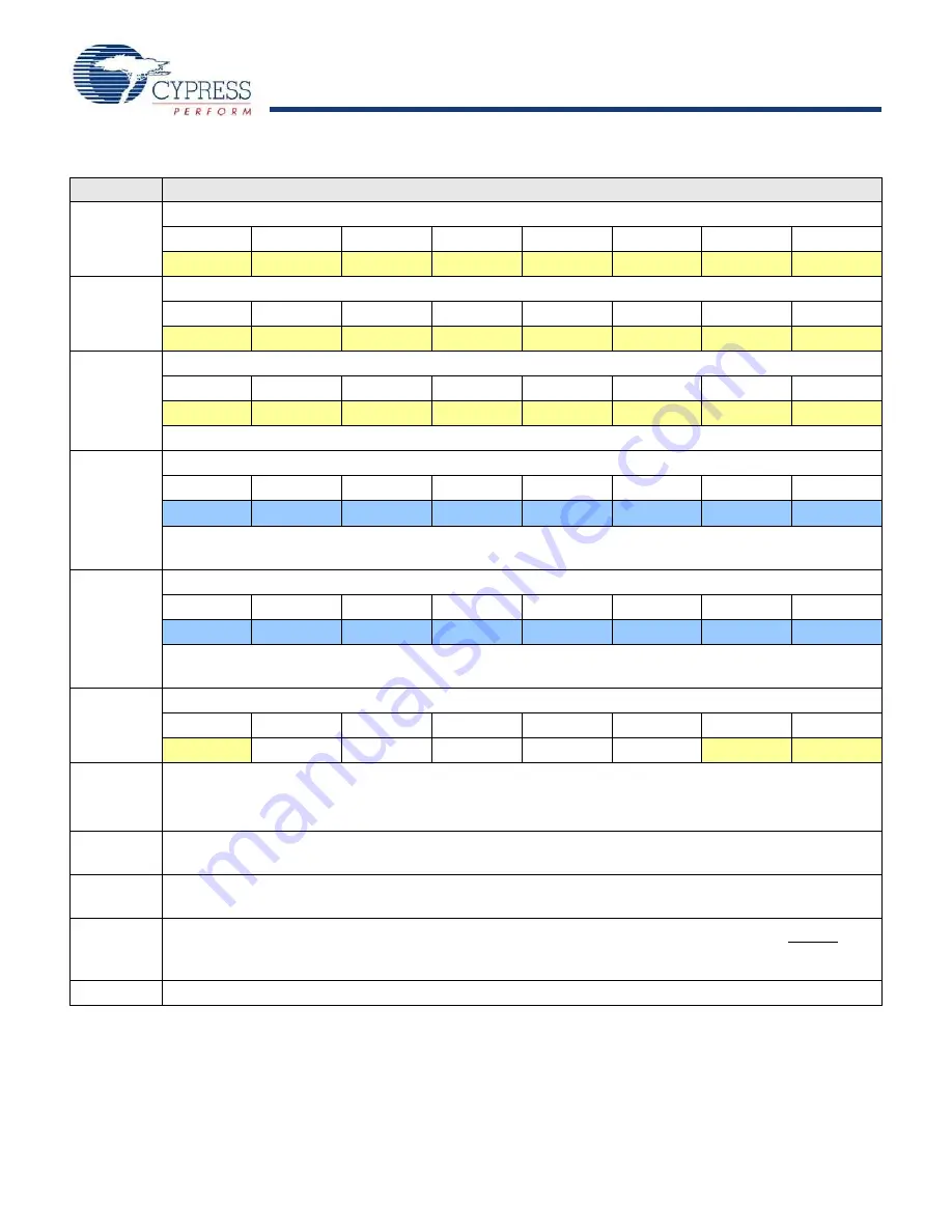
12h

Serial Number Byte 2

D7

D6

D5

D4

D3

D2

D1

D0

SN.23

SN.22

SN.21

SN.20

SN.19

SN.18

SN.17

SN.16

11h

Serial Number Byte 1

D7

D6

D5

D4

D3

D2

D1

D0

SN.15

SN.14

SN.13

SN.12

SN.11

SN.10

SN.9

SN.8

10h

Serial Number Byte 0

D7

D6

D5

D4

D3

D2

D1

D0

SN.7

SN.6

SN.5

SN.4

SN.3

SN.2

SN.1

SN.0

All serial number bytes are read/write when SNL = ‘0’, read-only when SNL = ‘1’. Nonvolatile.

0Fh

Event Counter Byte 1

D7

D6

D5

D4

D3

D2

D1

D0

EC.15

EC.14

EC.13

EC.12

EC.11

EC.10

EC.9

EC.8

Event Counter Byte 1. Increments on programmed edge event on CNT input. Nonvolatile when NVC = ‘1’, 
Battery-backed when NVC = ‘0’, read/write.

0Eh

Event Counter Byte 0

D7

D6

D5

D4

D3

D2

D1

D0

EC.7

EC.6

EC.5

EC.4

EC.3

EC.2

EC.1

EC.0

Event Counter Byte 0. Increments on programmed edge event on CNT input. Nonvolatile when NVC = ‘1’, 
Battery-backed when NVC = ‘0’, read/write.

0Dh

Event Counter Control

D7

D6

D5

D4

D3

D2

D1

D0

NVC

-

-

-

RC

WC

POLL

CP

NVC

Nonvolatile/Volatile Counter: Setting this bit to ‘1’ makes the counter nonvolatile and counter operates only when
V

DD

 is greater than V

TP

. Setting this bit to ‘0’ makes the counter volatile, which allows counter operation under

V

BAK

 or V

DD

 power. If the NVC bit is changed, the counter value is not valid. Nonvolatile, read/write. 

RC

Read Counter. Setting this bit to ‘1’ takes a snapshot of the two counter bytes allowing the system to read the
values without missing count events. The RC bit will be automatically cleared.

WC

Write Counter. Setting this bit to a ‘1’ allows the user to write the counter bytes. While WC = ‘1’, the counter is
blocked from count events on the CNT pin. The WC bit must be cleared by the user to activate the counter. 

POLL

Polled Mode: When POLL = ‘1’, the CNT pin is sampled for 30 µs every 125 ms. If POLL is set, the NVC bit is
internally cleared and the CP bit is set to detect a rising edge. The RTC oscillator must be enabled (OSCEN = ‘0’)
to operate in polled mode. When POLL = ‘0’, CNT pin is continuously active. Nonvolatile, read/write.

CP

The CNT pin detects falling edges when CP = ‘0’, rising edges when CP = ‘1’. Nonvolatile, read/write.

Table 7.  Register Description 

 (continued)

Address

Description

Summary of Contents for FM33256B

Page 1: ...ess mainly focus on the distribution of electronic components Line cards we deal with include Microchip ALPS ROHM Xilinx Pulse ON Everlight and Freescale Main products comprise IC Modules Potentiometer IC Socket Relay Connector Our parts cover such applications as commercial industrial and automotives areas We are looking forward to setting up business relationship with you and hope to provide you...

Page 2: ... 64 bit serial number area and general purpose comparator that can be used for a power fail NMI interrupt or any other purpose The FM33256B is a 256 Kbit nonvolatile memory employing an advanced ferroelectric process A ferroelectric random access memory or F RAM is nonvolatile and performs reads and writes similar to a RAM It provides reliable data retention for 151 years while eliminating the com...

Page 3: ...FM33256B Document Number 001 86213 Rev C Page 2 of 39 Logic Block Diagram ...

Page 4: ...able Latch 25 Status Register and Write Protection 26 RDSR Read Status Register 26 WRSR Write Status Register 26 RDPC Read Processor Companion 27 WRPC Write Processor Companion 27 Memory Operation 28 Write Operation 28 Read Operation 28 Maximum Ratings 30 Operating Range 30 DC Electrical Characteristics 30 Data Retention and Endurance 32 Capacitance 32 Thermal Resistance 32 AC Test Conditions 32 S...

Page 5: ...e This pin should be tied to ground if unused ACS Output Alarm Calibration SquareWave This is an open drain output that requires an external pull up resistor In normal operation this pin acts as the active low alarm output In Calibration mode a 512 Hz square wave is driven out In SquareWave mode the user may select a frequency of 1 512 4096 or 32768 Hz to be used as a continuous output The SquareW...

Page 6: ...escribed in more detail on page 26 Processor Companion In addition to nonvolatile RAM the FM33256B incorporates a real time clock with alarm and highly integrated processor companion The companion includes a low VDD reset a programmable watchdog timer a 16 bit nonvolatile event counter a comparator for early power fail detection or other purposes and a 64 bit serial number Processor Supervisor Sup...

Page 7: ...wing the FM33256B to filter and de bounce a manual reset switch The RST input detects an external low condition and responds by driving the RST signal LOW for 100 ms max This effectively filters and de bounces a reset switch After this timeout tRPU the user may continue pulling down on the RST pin but SPI commands will not be locked out Note The internal weak pull up eliminates the need for additi...

Page 8: ...the CNT pin and the other contact to the case chassis usually ground The typical solution uses a pull up resistor on the CNT pin and will continuously draw battery current The FM33256B chip allows the user to invoke a polled mode which occasionally samples the pin in order to minimize battery drain It internally tries to pull the CNT pin up and if open circuit will be pulled up to a VIH level whic...

Page 9: ... matches from setting AF but will not automatically clear the AF flag The RTC alarm is integrated into the special function registers and shares its output pin with the 512 Hz calibration and square wave outputs When the RTC calibration mode is invoked by setting the CAL bit register 00h bit 2 the ACS output pin will be driven with a 512 Hz square wave and the alarm will continue to operate Since ...

Page 10: ... is less than 2 5 V the RTC and event counters will switch to the backup power supply on VBAK The clock operates at extremely low current in order to maximize battery or capacitor life However an advantage of combining a clock function with FRAM memory is that data is not lost regardless of the backup power source The IBAK current varies with temperature and voltage see DC Electrical Characteristi...

Page 11: ...ments have the CALS sign bit set to 1 whereas negative ppm adjustments have CALS 0 After calibration the clock will have a maximum error of 2 17 ppm or 0 09 minutes per month at the calibrated temperature The user will not be able to see the effect of the calibration setting on the 512 Hz output The addition or subtraction of digital pulses occurs after the 512 Hz output The calibration setting is...

Page 12: ... 41 24 45 57 101010 11 511 9767 511 9744 45 58 49 91 101011 12 511 9744 511 9722 49 92 54 25 101100 13 511 9722 511 9700 54 26 58 59 101101 14 511 9700 511 9678 58 60 62 93 101110 15 511 9678 511 9656 62 94 67 27 101111 16 511 9656 511 9633 67 28 71 61 110000 17 511 9633 511 9611 71 62 75 95 110001 18 511 9611 511 9589 75 96 80 29 110010 19 511 9589 511 9567 80 30 84 63 110011 20 511 9567 511 9544...

Page 13: ...8 49 91 001011 12 512 0256 512 0278 49 92 54 25 001100 13 512 0278 512 0300 54 26 58 59 001101 14 512 0300 512 0322 58 60 62 93 001110 15 512 0322 512 0344 62 94 67 27 001111 16 512 0344 512 0367 67 28 71 61 010000 17 512 0367 512 0389 71 62 75 95 010001 18 512 0389 512 0411 75 96 80 29 010010 19 512 0411 512 0433 80 30 84 63 010011 20 512 0433 512 0456 84 64 88 97 010100 21 512 0456 512 0478 88 9...

Page 14: ...arm Minutes 00 59 19h M Alarm 10 seconds Alarm seconds Alarm Seconds 00 59 18h SNL AL SW F1 F0 VBC FC VTP1 VTP0 Companion Control 17h Serial Number Byte 7 Serial Number 7 FFh 16h Serial Number Byte 6 Serial Number 6 FFh 15h Serial Number Byte 5 Serial Number 5 FFh 14h Serial Number Byte 4 Serial Number 4 FFh 13h Serial Number Byte 3 Serial Number 3 FFh 12h Serial Number Byte 2 Serial Number 2 FFh ...

Page 15: ...Hex Value Address Hex Value Address Hex Value 1Dh 0x81 12h 0x00 05h 0x00 1Ch 0x81 11h 0x00 04h 0x00 1Bh 0x80 10h 0x00 03h 0x00 1Ah 0x80 0Fh 0x00 02h 0x00 19h 0x80 0Eh 0x00 01h 0x00 18h 0x40 0Dh 0x01 00h 0x80 17h 0x00 0Ch 0x00 16h 0x00 0Bh 0x00 15h 0x00 08h 0x00 14h 0x00 07h 0x00 13h 0x00 06h 0x00 ...

Page 16: ...s bit to 1 causes the match circuit to ignore the Hours value Battery backed read write 1Ah Alarm Minutes D7 D6 D5 D4 D3 D2 D1 D0 M 10 min 2 10 min 1 10 min 0 Min 3 Min 2 Min 1 Min 0 Contains the alarm value for the minutes and the mask bit to select or deselect the Minutes value M Match Setting this bit to 0 causes the Minutes value to be used in the alarm match logic Setting this bit to 1 causes...

Page 17: ...VBAK Clearing VBC to 0 disables the charge current Battery backed read write VTP 1 0 VTP Select These bits control the reset trip point for the low VDD reset function Nonvolatile read write VTP VTP1 VTP0 2 60 V 0 0 factory default 2 75 V 0 1 2 90 V 1 0 3 00 V 1 1 17h Serial Number Byte 7 D7 D6 D5 D4 D3 D2 D1 D0 SN 63 SN 62 SN 61 SN 60 SN 59 SN 58 SN 57 SN 56 16h Serial Number Byte 6 D7 D6 D5 D4 D3...

Page 18: ...Counter Setting this bit to 1 makes the counter nonvolatile and counter operates only when VDD is greater than VTP Setting this bit to 0 makes the counter volatile which allows counter operation under VBAK or VDD power If the NVC bit is changed the counter value is not valid Nonvolatile read write RC Read Counter Setting this bit to 1 takes a snapshot of the two counter bytes allowing the system t...

Page 19: ...s independent leading and trailing edges start and end of window to be set New watchdog timeouts are loaded when the timer is restarted by writing the 1010b pattern to WR 3 0 To save power disable timer circuit the EndTime may be set to all zeroes Nonvolatile read write Watchdog EndTime WDET4 WDET3 WDET2 WDET1 WDET0 Disables Timer 0 0 0 0 0 min max 60 ms 200 ms 0 0 0 0 1 120 ms 400 ms 0 0 0 1 0 18...

Page 20: ...og Restart Writing a pattern 1010b to WR 3 0 restarts the watchdog timer The upper nibble contents do not affect this operation Writing any pattern other than 1010b to WR 3 0 has no effect on the watchdog Write only 09h Watchdog Flags D7 D6 D5 D4 D3 D2 D1 D0 EWDF POR LB EWDF Early Watchdog Timer Fault Flag When a watchdog restart occurs too early before the programmed watchdog StartTime the RST pi...

Page 21: ...Month Month 3 Month 2 Month 1 Month 0 Contains the BCD digits for the month Lower nibble contains the lower digit and operates from 0 to 9 upper nibble one bit contains the upper digit and operates from 0 to 1 The range for the register is 1 12 Battery backed read write 06h Timekeeping Date of the month D7 D6 D5 D4 D3 D2 D1 D0 0 0 10 date 1 10 date 0 Date 3 Date 2 Date 1 Date 0 Contains the BCD di...

Page 22: ... On a power up without a VBAK source or on a power up after a VBAK source has been applied this bit is internally set to 1 which turns off the oscillator Battery backed read write AF Alarm Flag This bit is set to 1 when the time and date match the values stored in the alarm registers with the Match bit s 0 The user must clear it to 0 Battery backed internally set user must clear bit CF Century Ove...

Page 23: ... user registers The user can then read them without concerns over changing values causing system errors The R bit going from 0 to 1 causes the timekeeping capture so the bit must be returned to 0 prior to reading again Battery backed read write Reserved Reserved bits Do not use Should remain set to 0 Table 7 Register Description continued Address Description ...

Page 24: ...es Chip Select CS To select any slave device the master needs to pull down the corresponding CS pin Any instruction can be issued to a slave device only while the CS pin is LOW When the device is not selected data through the SI pin is ignored and the serial output pin SO remains in a high impedance state Note A new instruction must begin with the falling edge of CS Therefore only one opcode can b...

Page 25: ...is available on the falling edge of SCK The two SPI modes are shown in Figure 15 on page 24 and Figure 16 on page 24 The status of the clock when the bus master is not transferring data is SCK remains at 0 for Mode 0 SCK remains at 1 for Mode 3 The device detects the SPI mode from the status of the SCK pin when the device is selected by bringing the CS pin LOW If the SCK pin is LOW when the device...

Page 26: ...it in the Status Register has no effect on the state of this bit only the WREN opcode can set this bit The WEL bit will be automatically cleared on the rising edge of CS following a WRDI a WRSR a WRPC or a WRITE operation This prevents further writes to the Status Register or the F RAM array without another WREN command Figure 17 illustrates the WREN command bus configuration WRDI Reset Write Enab...

Reviews: