


2RT0435T
Target Description and Application Manual
www.IGBT-Driver.com
Page 13
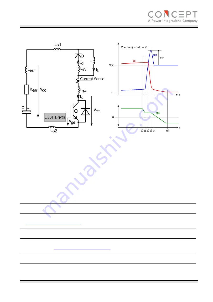
Fig. 10 Test circuit (left) and typical switching behavior (right)
Legend to Fig. 10
t0 = Initiation of the turn-off process
t1 = Start of turn-off time
t2 = Start of collector current fall time
t3 = Maximum collector voltage
t4 = IGBT is blocking, start of tail current
t5 = End of tail current
In comparison with other driving methods, active clamping allows enhanced utilization of the IGBT modules
during normal operation by increasing the switching speed and therefore reducing switching losses. The
overvoltage at fault-current turn-off is also managed by active clamping. For the maximum permitted DC-link
voltage, refer to the Base Board data sheets /4/.
Parallel connection of 2RT0435T
If parallel connection of 2RT0435T Base Boards is required, please refer to the application note AN-0904 /7/
on
www.IGBT-Driver.com/go/app-note
and to /6/.
3-level and multilevel topologies
If the 2RT0435T Base Boards are to be used in 3-level or multilevel topologies, please refer to the application
note AN-0901 /8/ on
www.IGBT-Driver.com/go/app-note
.
Low-inductance layout
The active-clamping function should not lead anyone to forget about the inductances of the power stack. For
several reasons, it is recommended to reduce the DC-link stray inductance to about 30nH…100nH depending
on the IGBT modules used with 2RT0435T Base Boards.