background image

30

D026227_08 CR822x Single Board Decoded Scan Engine Integration Guide

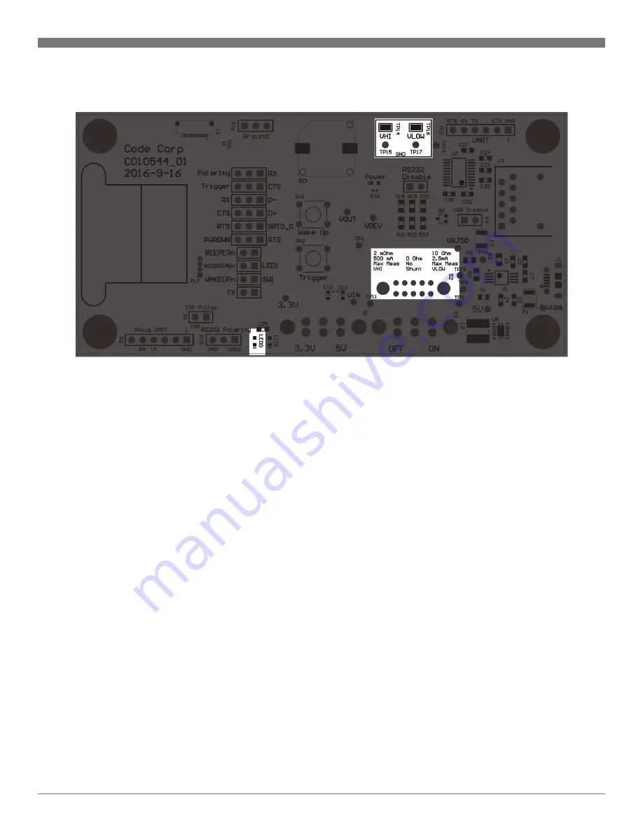
The development board provides current shunt amplifiers for two different 
ranges to perform power measurements on the engine. Switch S2 will 
select which path the current to the engine is routed.

The center position of S2 has no shunt, and directly connects VDEV (the 
voltage selected by S1, 3.3V or 5V) to VOUT (the voltage to the engine 
provided through J2).

Using an oscilloscope capable of math functions, such as the Keysight 
InfiniiVision MSOX3104T, and two voltage probes, the engine’s power can 
be easily measured in the operating and sleep states. Measure VOUT and 
multiply with the calculated current to get power.

Operating Current

The left position of S2, closest to the engine, has a 2mΩ shunt between 
VDEV and VOUT. The shunt has an integrated current shunt amplifier 
that provides a factory calibrated gain of 2.0V/A. The voltage output of 
this amplifier can be read from VHI on TP14 or TP15. To convert from 
the voltage output to a current, divide the output by 2. This amplifier is 
capable of measuring up to 500mA with a max VHI of 5V.

Sleep Current

To measure the current when the engine is asleep, first the offset of 
the system needs to be measured. Disconnect the engine from the 
development board by disconnecting the ribbon cable from J2. Turn on 
the development board, set the desired voltage on S1, then set S2 in the 
rightmost position closest to the RJ50 connector. Use a multimeter or 
oscilloscope to measure the VLOW voltage on TP16 or TP17. This voltage 
is the offset of the measurement. 

To perform a sleep current measurement, start with S2 in either the left 
or center position. Wait until the engine sleeps or put it to sleep. LED0 
will be off if the engine is asleep and on if it is awake. When the engine 
is asleep, move S2 to the right position closest to the RJ50 and USB 
connectors. This will route the current to the engine through a 10Ω shunt 
attached to a current shunt amplifier with a gain of 100V/V. The output 
of the amplifier can be read from VLOW on TP16 or TP17. To convert 
from voltage to current, subtract the offset you measured earlier from 
VLOW and divide by 1000. The silkscreen on Rev 01 PCB’s does not 
show the correct formula or range. The max range for the low current path 
measurement is 5mA with a max VLOW of 5V.

Note: The silkscreen on Rev 01 PCB’s does not show the correct formula 
or range.

9.3 – Power Measurements

Summary of Contents for Code Reader 822 Series

Page 1: ...CR822x Single Board Decoded Scan Engine INTEGRATION GUIDE Configuration Guide www codecorp com YouTube com codecorporation MANUAL VERSION 08 RELEASE DATE JANUARY 2018 HIROS...

Page 2: ...onsequential damages resulting from the furnishing performance or use of this material Code Corporation does not assume any product liability arising out of or in connection with the application or us...

Page 3: ...erface Pinouts CR8222 RS232 13 4 4 Host Interface Pinouts CR8221 USB 13 4 5 Electrical Control Signals 14 4 6 Power Modes 14 4 7 Power On Boot Timing Diagram 15 4 8 Power Down Timing Diagram 16 4 9 Sl...

Page 4: ...Kiosks and more 1 1 Product Overview 1 CR822x Introduction The following table describes the options available for the CR822x engine Any SKU Part Number can be built using the following table SKU CR8...

Page 5: ...Red LED Illumination Lens 3 Lens 4 Self Tapping Screw Holes 5 a Illumination Board b Imager Board 6 Connector Receptacle 30 pin 0 4 mm pitch 4 3 5a 2 5b 2 4 6 1 1 Blue LED Targeting Lens 2 Red LED Il...

Page 6: ...079 2 50 mm 098 Length B Mounting Substrate Thickness A 2 00 mm Mounting Substrate Thickness A 2 50 mm Torque N A 1 5 Ibf in 807 20 50 FRONT VIEW 536 13 63 SIDE VIEW 138 3 50 512 13 00 A 1 65 065 3 00...

Page 7: ...g screw with the following dimensions Minimum Maximum Thread Engagement 2 00 mm 079 2 50 mm 098 Length B Mounting Substrate Thickness A 2 00 mm Mounting Substrate Thickness A 2 50 mm Torque N A 1 5 Ib...

Page 8: ...2 20 087 HIGH 2X 3 00 118 2X 1 70 067 2X 0 95 037 2X 2 25 089 1 20 047 2 25 089 2 00 079 TOP BOTTOM 2 00 079 80 031 KEEP OUT 1 50 059 HIGH 20 50 807 MOLEX 501745 0301 PIN 1 TO SCAN ENGINE 0 80 031 1 7...

Page 9: ...at the processor does not exceed 100 C The enclosure should minimize infiltration by airborne contaminants and foreign materials 2 The CR822x must not come in contact with water 3 The CR822x is sensi...

Page 10: ...acrylic Thickness 1 mm or less If your design constraints prevent the window from being mounted within 0 5 mm of the face of the engine Code recommends an anti reflective AR coating be applied to both...

Page 11: ...de 39 40 51 00 X Y 5 118 130 00 FOCAL DISTANCE 3 2 Imager Field of View CR822x Field of View Diagram The Field of View for the CR822x for Horizontal and Vertical positioning of the imager is shown bel...

Page 12: ...in length can be used with a 0 28 mm 011 trace width and 0 3 mm trace thickness Longer cables can be used at higher voltages Power Sequencing There is no special power sequence needed for the CR822x a...

Page 13: ...2 Request to Send TTL level 1 8 PwrDwn Output Power down indicator 1 9 nBeeper Output Feedback indicator success error etc active low 1 10 nGoodRead Output Indicates a successful decode active low 1 1...

Page 14: ...LOW pulse Note that nWakeUp must be HIGH when the CR822x enters the sleep state in order for nWakeUp to awaken the CR822x on assertion Also note that when the sleep state is not being used this pin s...

Page 15: ...ming Diagram The PwrDwn signal will transition to HIGH shortly after Vin is applied and will remain HIGH until the reader is ready Parameter Symbol Min Typical Max Unit Time from Power On to firmware...

Page 16: ...Outputs PwrDwn nGoodRead nBeeper Signal Description Min Typical Max Unit Twupw nWakeUp pulse width 10 10 msec Twu Time between nWakeUp asserted and CR822x ready 10 11 12 msec Tready Time between CR822...

Page 17: ...gger Accepted to Image Capture Complete Tic 5 32 100 msec 1 Minimum Trigger duration Ttmin 10 20 N A 2 Trigger Confirmation Time Ttct 0 0 see note msec 3 TTMIN TTCT TRIGGER ACCEPTED IMAGE CAPTURE COMP...

Page 18: ...h 2 0 V Low level input voltage Vil 0 8 V High level output voltage Voh 2 4 Vin 1 Low level output voltage Vol 0 55 V Active operating current Ia 475 mA 2 5 Sleep current Is 150 uA 3 4 Inrush current...

Page 19: ...put Hsync from imager 12 Gnd Power Power and signal ground 13 Dout4 Input Imager pixel data 4 14 Dout5 Input Imager pixel data 5 15 Dout6 Input Imager pixel data 6 16 Dout7 Input Imager pixel data 7 1...

Page 20: ...aight 2 of 5 Telepen Trioptic UPC EAN JAN Stacked 1D Barcodes Codablock F Code 49 GS1 Composite CC A CC B CC C MicroPDF PDF417 2D Barcodes Aztec Code Data Matrix Han Xin MaxiCode Micro QR Code QR Code...

Page 21: ...r the specified barcodes Test Barcode Min mm inches Max mm inches 7 5 Mil Code 39 2 0 50 9 6 245 10 5 Mil GS1 Databar 1 4 35 8 9 225 13 Mil UPC 1 6 40 14 6 370 5 8 Mil PDF417 3 3 85 6 1 155 6 7 Mil PD...

Page 22: ...ate or other work around is provided assumes the remaining warranty of the original Code Product and does not extend the duration of the original warranty period Software and Data Code is not responsi...

Page 23: ...the development board via J23 Trigger Wake Up Switches SW1 and SW2 allow the user to wake the unit from Sleep Mode and trigger a barcode read respectively If the unit is in a sleep state when the tri...

Page 24: ...RX RX D LED0 D LED1 RTS TX TRIGGER TRIGGER WAKE UP LED1 BEEPER LED0 RTS CTS SW1 WAKE UP SW2 TRIGGER EXPANDED ILLUMINATION VPI Engineering C005425_02 pcb 20 May 2010 TX RX POLARITY CTS POLARITY BOOT S...

Page 25: ...RTS CTS SW1 WAKE UP SW2 TRIGGER EXPANDED ILLUMINATION VPI Engineering C005425_02 pcb 20 May 2010 TX RX POLARITY CTS POLARITY BOOT SELECT RX J2 D1 J5 J6 F1 J19 J24 J3 U1 SPK1 U2 Serial Polarity and Boo...

Page 26: ...N but for different connection options The standard cables provide VIN through the RJ 50 connector J1 The fuse that protects the circuit when using the J1 connection is F2 F2 is located on the back si...

Page 27: ...all documentation required to quickly evaluate and integrate the CR82XX Scan Engine Scan Engine The development kit comes with a complete Decoded Scan Engine which includes the imager and decoder boa...

Page 28: ...be used for communication However if power is connected to the RJ50 cable the development board will select it as the power source over micro USB P12 provides a header to connect an FTDI cable for RS2...

Page 29: ...consistent power source to the engine For the CR8221 the switch must be set at 5V For the CR8222 the switch must be set at 3 3V The S3 switch turns the system on The S2 switch is used to select which...

Page 30: ...Sleep Current To measure the current when the engine is asleep first the offset of the system needs to be measured Disconnect the engine from the development board by disconnecting the ribbon cable f...

Page 31: ...efore performing a barcode read The development board includes a speaker BZ1 for audible indication as well as two LED s for visual indication LED0 connects to PWRDWN and is on when the engine is awak...

Page 32: ...umper block located just to the right of the engine configures the signals between the CR82xx and RJ 50 FTDI and USB connector This is done by shorting pins 1 2 or 2 3 on each jumper Refer to figures...

Page 33: ...r P15 selects whether or not the primary RS 232 data are inverted The RS 232 data will be inverted if P15 has pins 1 2 bridged GND and the center pin The CR82XX engines have an internal pullup on the...

Reviews: