— 18 —
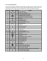
KEY TOUCH LSI (LSI6: TC190C020AF-001)
By counting the time between first-key input signal FI and second-key SI from the keyboard unit, the key
touch LSI detects key velocity of 256-step. Then the LSI sends the CPU the note number and its velocity
data.
Pin No.
Terminal
In/Out
Function
1
WRB
In
Write signal from CPU.
2 ~ 11, 13,
D0 ~ D15
In/Out
Data bus.
14, 16 ~ 19
12
VSS
In
Ground terminal (0 V).
15
VDD
In
VDD (5 V) source.
20 ~ 23
CA0 ~ CA3
In
Address bus.
24
VSS
In
Ground terminal (0 V).
25 ~ 32,
FI0 ~ FI4,
In
Key input signal.
34, 35
SI0 ~ SI4
33
VDD
In
VDD (5 V) source.
36 ~ 38,
KC0 ~ KC7
Out
Key scan signal.
40 ~ 44
39
VSS
In
Ground terminal (0 V).
45
VDD
In
VDD (5 V) source.
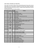
46 ~ 51
FI5 ~ FI7
In
Key input signal.
SI5 ~ SI7
52
VSS
In
Ground terminal (0 V).
53 ~ 58,
FI8 ~ FI10
60 ~ 62
SI8 ~ SI10
In
Key input signal (Not used).
KI0 ~ KI2
59
VDD
In
VDD (5 V) source.
63, 64
MODE0, MODE1
—
Not used.
65
VSS
In
Ground terminal (0 V).
66
KCKI
In
Clock signal for key common/input.
67 ~ 72,
—
Not used.
74 ~ 77
73
VDD
In
VDD (5 V) source.
78
RESB
In
Reset signal from CPU.
79
CSB
In
Chip selection signal.
80
RDB
In
Read signal from CPU.
Summary of Contents for WK-1800
Page 30: ...29 PRINTED CIRCUIT BOARD Main PCB JCM733 MA1M Top View Bottom View 1 6 5 4 3 2 9 10...
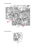
Page 31: ...30 Sub PCB JCM733 MA2M 7 8 Sub PCB JCM733 MA3M Top View Top View...
Page 32: ...31 Console PCBs JCM733 CN1M Top View Top View Console PCBs JCM733 CN2M...
Page 33: ...32 Display PCB JCM733 LCD1M Top View Bottom View...
Page 34: ...33 Keyboard PCBs JCM763T KY1M Top View Top View Keyboard PCBs JCM763T KY2M...
Page 40: ...39 SubPCB JCM733 MA2M MA3M 7 8 Regulator IC Power Amp...
Page 41: ...40 Console PCBs JCM733 CN1M CN2M S Register S Register...
Page 42: ...41 LCD Driver PCB JCM733 LCD1M LCD Driver Back Light Circuit...

