background image

— 23 —

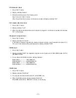
 Pitch Bender check

1. Press “CH12” button.

2. Display indicates “Bender”.

3. Rotate the pitch bender to the following order

Max 

 Center 

 Min 

 Center

When the pitch bender is proper, an OK alarm sounds and display indicates "OK".

 AC adaptor detection check.

1. Press “CH14” button.

2. DIsplay indicates "Jack".

3. When the instrument detects that an AC adaptor is plugged in, an OK alarm sounds and indicates

“OK” on the display.

 Keyboard and pedal check

1. Press “CH10” button.

2. Display indicates “Tch & Pd1”.

In accordance with key, depressions, display indicates velocity value (hexadecimal values 01 to
127), and in accordance with pedal depressions, display indicates "SUS".

 ROM check

1. Press “CH2” button.

2. Display indicates "ROM", the diagnostic program counts check sums of 1Mbit ROM(inside of CPU)

and 64Mbit ROMs.

3. In accordance with ROMs functions, display indicates;

“ROM H80K” --------------- 1Mbit ROM OK
“ROM 64MOK” ------------- 64Mbit ROMs OK
“ROM H8NG” -------------- 1Mbit ROM NG
“ROM 64MNG” ------------ 64Mbit ROMs NG

 RAM check

1. Press “CH15” button.

2. Display indicates "RAM Test".

3. The program executes write/read test in all the RAM area.

4. When the RAM is proper, display indicates “RAM OK”.

If the RAM malfunctions, “RAM NG” is shown on the display.

Summary of Contents for WK-1800

Page 1: ...ORD SONG FINGERED PATTERN EXTERNAL INTERNAL UPPER1 CH 1 UPPER2 CH 2 LOWER1 CH 3 LOWER2 STORE BANK CH 4 ACC VOL CH 5 CHORD1 CH 6 CHORD2 CH 7 CHORD3 CH 8 BASS CH 9 RHYTHM CH 10 TR1 CH 11 TR2 CH 12 TR3 C...

Page 2: ...ONTENTS Specifications 2 Important Operation 4 Block Diagram 5 Circuit Description 6 Diagnostic Program 22 Major Waveformes 28 Printed Circuit Board 29 Exploded View 34 Parts List 35 Schematic Diagram...

Page 3: ...sequencer Songs 2 Recording tracks 6 2 through 6 are melody tracks Recording method Real time Memory capacity total for two songs Approximately 8 000 notes Punch in Supported Pattern sequencer Number...

Page 4: ...AC adapter AD 12 Auto power off Turns power off approximately six minutes after last key operation En abled under battery power only can be disabled manually Speaker output 5 W 5 W Power consumption...

Page 5: ...make figures easier to read from any viewing angle Within five seconds after pressing the CONTRAST button press to increase the contrast value mak ing the display darker or to decrease it making the d...

Page 6: ...r TC74HC164 IC401 LCD FDD Controller HD63266F LSI10 3 5 FDD Unit DF354H064C Back up Power CR2032 Power Supply Circuit IC202 Q207 Q208 Q211 Q214 Q215 Q209 Q213 CPU HD6433048SA89F LSI9 Working RAM TC552...

Page 7: ...42 C 42 D42 D 42 E42 F42 F 42 FI5 G41 G 41 A41 A 41 B41 C51 C 51 D51 SI5 G42 G 42 A42 A 42 B42 C52 C 52 D52 FI6 D 51 E51 F51 F 51 G51 G 51 A51 A 51 SI6 D 52 E52 F52 F 52 G52 G 52 A52 A 52 FI7 B51 C61...

Page 8: ...P TEMPO TEMPO MIXER SELECT NO YES PWSW POWER TRANSPOSE TRANSPOSE AUTO HARMONIZE KC0 KC1 KC2 KC3 KC4 KC5 KC6 KC7 KI0 MODE RECORD SONG PATTERN DSP KI2 UPPER1 CH1 UPPER2 CH2 LOWER1 CH3 LOWER2 CH4 ACC VOL...

Page 9: ...9 LSI3 Working RAM 7 256 kbit LSI4 Internal Memory ROM1 5 32 Mbit LSI1 RAM2 2 1 Mbit LSI8 ROM2 6 32 Mbit LSI2 VDD Battery set RESET CPU HD6433048SA89F LSI9 FDD Controller HD63266F LSI10 RESET Power Su...

Page 10: ...aptor is set Other voltages are controlled by APO Auto Power Off signal from CPU The regulator IC BA9700A generates square waveform from pin 5 as PWM Pulse Wide Modulation The LC filter makes stable o...

Page 11: ...it BOK EA0 EA14 D0 D15 ED0 ED15 KC0 KC7 SI0 SI9 FI0 FI9 RA0 RA21 RA0 RA21 CS RA23 CE OE A0 A20 NC Q0 Q15 CE OE A0 A20 NC Q0 Q15 WE OE D0 D15 A0 A14 PG 24 576 MHz DAC LOUT ROUT SORP Sound data BOK Bit...

Page 12: ...ation speed 360 Min 1 rpm 1 5 FDD Interface Host system Drive CN2 connector Index 8 Density Select 4 Drive Select 1 12 Motor ON 16 Direction 18 Step 20 Write Data 22 Write Gate 24 Track 00 26 Write Pr...

Page 13: ...BACKLIGHT When voltage CVDD is supplied transistors Q601 and Q602 start oscillation From the oscillation voltage transformer T601 generates about 600 V which is necessary for lighting the backlight D...

Page 14: ...Not used 61 CLKOUT Out Clock signal 16 MHz 62 STBY Not used 63 RES In Reset signal at VDD 5 V supplied 64 NMI In Power ON signal input 65 VSS In Ground terminal 0 V 66 67 EXTAL XTAL In Clock 16 MHz i...

Page 15: ...p select signal for FDD 89 CS2 Out Acknowledge signal FDD DMA function 90 CS1 Out Chip select signal for Key controller 91 CS0 Out Chip select signal for DSP 92 VSS In Ground terminal 0 V 93 TEND0 Out...

Page 16: ...TCKB Not used 16 VCC1 In 5 V source 17 GND1 In Ground 0 V source 18 19 XT0 XT1 In Out 24 576 MHz clock input output Connected to a crystal oscillator 20 SGL In System control terminal Single chip syst...

Page 17: ...ata bus 20 DREQ In Request signalof DMA 21 IRQ Not used 22 DEND In End signal for data transfer 23 VSS3 In Ground terminal 0 V 24 1 2 EX1 Not used 25 VCC1 In DVDD 5 V source 26 27 28 NUM1 NUM2 Not use...

Page 18: ...42 VSS4 VSS5 In Ground terminal 0 V 43 NC Not used 44 46 VCC2 VCC3 In DVDD 5 V source VCC4 47 WGATE Out Write gate signal to FDD 48 WDATA Out Write data signal to FDD 49 VSS6 In Ground terminal 0 V 50...

Page 19: ...In Address bus 24 VSS In Ground terminal 0 V 25 32 FI0 FI4 In Key input signal 34 35 SI0 SI4 33 VDD In VDD 5 V source 36 38 KC0 KC7 Out Key scan signal 40 44 39 VSS In Ground terminal 0 V 45 VDD In V...

Page 20: ...age input 26 30 V1 V5 In Those voltages are used for generating the stepped pulse of the LCD drive signals 31 32 LP XSCL Not used 33 VDD In LVDD 5 V source 34 35 FR DO Not used 36 RS In Data command d...

Page 21: ...und 2 D GND In Ground 0 V source for internal digital circuit 3 Bit SEL Not used 4 DVDD In 5 V source for internal digital circuit 5 A GND In Ground 0 V source for internal analog circuit 6 R OUT Out...

Page 22: ...1 OUT2 OUT2 PER GND1 PWR GND2 Output amplifier Output amplifier Input amplifier Input amplifier CH 1 CH 2 Ripple Filter Starting Time Vcc ground shorting protection circuit Load shorting protection ci...

Page 23: ...H PRESET button 8 MIXER SELECT button 9 CHANNEL button CH1 10 CH2 11 CH3 12 CH4 13 CH5 14 CH6 15 CH7 16 CH8 17 CH9 18 CH10 19 CH11 20 CH12 21 CH13 22 CH14 23 CH15 24 CH16 25 SPLIT button 26 LAYER butt...

Page 24: ...Pd1 In accordance with key depressions display indicates velocity value hexadecimal values 01 to 127 and in accordance with pedal depressions display indicates SUS ROM check 1 Press CH2 button 2 Displ...

Page 25: ...e sound from the left speaker and indicates sound L on the display Large sound right channel output 1 Press CH9 button 2 The instrument emits a large volume sound from the right channel and indicates...

Page 26: ...te in the following order with verification sound a FULL RANGE CHORD b FINGERED c CASIO CHORD d SONG e PATTERN f FREE SESSION g SYNTH h DISK FDD test 1 Press DISK button 2 Display indicates Dsk0 9E wh...

Page 27: ...itializes the instrument Pressing button invalidates system reset 4 The instrument turns on automatically Touch off max 1 While pressing down RHYTHM and MODE buttons turn the power on 2 Display indica...

Page 28: ...ring reading from the disk Disk is full Not enough memory to perform the process No memory is available to load data An attempt was made to play data that is not SMF FORMAT 0 An attempt was made to ac...

Page 29: ...signal RES IC5 pin 1 1 2 3 4 5 NMI signal LSI9 pin 64 6 Reset signal RESB LSI9 pin 87 7 Sound signal L OUT SIELD WIRE PE W 8 Sound signal L VOL0OUT JJ connector pin 1 Tone Grand Piano No 000 Volume M...

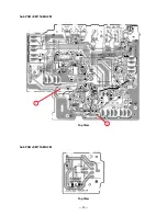
Page 30: ...29 PRINTED CIRCUIT BOARD Main PCB JCM733 MA1M Top View Bottom View 1 6 5 4 3 2 9 10...

Page 31: ...30 Sub PCB JCM733 MA2M 7 8 Sub PCB JCM733 MA3M Top View Top View...

Page 32: ...31 Console PCBs JCM733 CN1M Top View Top View Console PCBs JCM733 CN2M...

Page 33: ...32 Display PCB JCM733 LCD1M Top View Bottom View...

Page 34: ...33 Keyboard PCBs JCM763T KY1M Top View Top View Keyboard PCBs JCM763T KY2M...

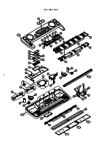
Page 35: ...34 EXPLODED VIEW 41 30 29 33 34 35 36 37 31 32 38 40 40 39 4 7 9 8 3 28 1 43 23 27 42 26 26 23 27 22 46 44 45 50 47 48 50 49 49 11 12 20 21 19 25 6 10 R 1 24 5 R 2 R 5 R 4 R 5 R 3 18 16 17 14 13 15 2...

Page 36: ...our spare parts department if you need these parts for refurbish 1 Prices and specifications are subject to change with out prior notice 2 As for spare parts order and supply refer to the GUIDEBOOK fo...

Page 37: ...77 T 5 AA C D203 D211 23901463 DIODE SCHOTTKY SB20 03B 2 AD C D205 D206 23901344 DIODE 1SS133T 77 T 2 AA C N D209 D210 10025045 DIODE ZENER MTZJT 777 5B 2 AA C D213 23601085 DIODE ZENER HZS6B1L TD 1 A...

Page 38: ...el N 23 10025062 PORT SPEAKER M241300 1 2 AD X N 24 10025077 BND ASS Y TK M340804 4 M732 1 BV C Bender N 25 10025078 BND ASS Y TK M340804 5 M732 1 BU C Modulation 26 38311105 SPEAKER S12J96A 2 BM C Wo...

Page 39: ...38 SCHEMATIC DIAGRAMS MainPCB JCM733 MA1M ROM1 ROM2 6 5 DSP Working RAM Reset IC CPU FDD Controloer Backup Power RAM2 RAM1 Key Controller D A Converter 4 3 1 2 10 9...

Page 40: ...39 SubPCB JCM733 MA2M MA3M 7 8 Regulator IC Power Amp...

Page 41: ...40 Console PCBs JCM733 CN1M CN2M S Register S Register...

Page 42: ...41 LCD Driver PCB JCM733 LCD1M LCD Driver Back Light Circuit...

Page 43: ...42 Keyboard PCBs JCM763T KY1M KY2M...

Page 44: ...CASIO COMPUTER CO LTD Overseas Service Division 6 2 Hon machi 1 Chome Shibuya ku Tokyo 151 8543 Japan Ver 1 Apr 2007 Correction of the CIRCUIT DESCRIPTION P6...

Reviews: