background image

— 5 —

KEY TOUCH LSI(HG52E35P)

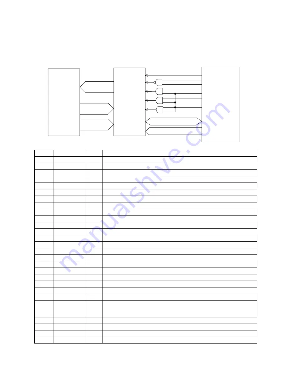
By counting the time between the first key input signal FI and the second SI from the keyboard unit, the key
touch LSI detects key velocity of 256-step. Then the LSI sends the CPU note numbers and their velocities.

Pin No.

Terminal

In/Out

Function

1

REQB

Out

Interrupt request. Not used.

2,3

FI10,SI10

In

Connected to +5V.

4

VCC

In

+5V source.

5

CRDB

In

Read enable signal.

6

CWRB

In

Write enable signal.

7

CCBB

In

Chip select signal.

8

T

In

Test terminal. Connected to +5V.

9

STYB

In

Standby terminal. Connected to +5V.

10

RESB

In

Reset signal.

11

W

In

Test terminal. Connected to +5V.

12

CKI

In

External clock input.

13

TMD

In

Test terminal. Connected to ground.

14

TST

In

Test terminal. Connected to ground.

15

CKO

Out

External clock output. Not used.

16

GND

In

Ground(0V) source.

17

XIN

In

Clock pulse input. Connected to ground.

18

XOUT

Out

Clock pulse output. Not used.

19

TRES

In

Test terminal. Connected to ground.

20~28

CD0~CD7

In/Out Data bus.

24

GND

In

Ground(0V) source.

29~31

CA0~CA2

Out

Address bus.

32

VCC

In

+5V source.

33~43

33~43
53~55

53~55
57~63

57~63

FI0~FI9

FI0~FI9

SI0~SI9

SI0~SI9

In

Key input signal.

40

VCC

In

+5V source.

44~53

KC0~KC7

Out

Key scan signal.

48,56

GND

In

Ground(0V) source.

54

VCC

In

+5V source.

Keyboard

KC0~KC7

FI0~FI9

SI0~SI9

Key Touch LSI
   HG52E35P

RESB

CCSB

CWRB

CRDB

CKI

P30/D0~P37/D7

P12/A2~P10/A0

CA0~CA2

CD0~CD7

D0~D7

A0~A2

         CPU
HD6433298A16P

P52/SCK

A12

A14

P44/-WR
P42/IRQ0
P43/-RD

P46/PHI

Summary of Contents for CTK-650

Page 1: ...with price CTK 650 ELECTRONIC KEYBOARD R CTK 650...

Page 2: ...8 329 3 DIGITAL SIGNAL PROCESSOR LSI S HG51A115A01FD 4 KEY TOUCH LSI HG52E35P 5 POWER AMPLIFIER LA4598 6 BUTTON MATRIX KEY MATRIX 8 WIRING DIAGRAM IC LEAD IDENTIFICATION AND INTERNAL CIRCUIT 10 PCB VI...

Page 3: ...SHIFTER ORGAN SP ENHANCER FLANGER EQLOUNDNESS DEMO tunes 3 tunes Other functions Transpose F C F half note Tuning adjustable A4 440KHz 50 cents increments Volume control Main Accompaniment Speakers 12...

Page 4: ...7 Segment LED LO0 LO4 LED driver BA612 La Lp KO0 KO5 Buttons KI1 KI7 100K VDD Power Switch MIDI IN OUT RAM 2 64K MN4464 08L 2 EA0 EA12 ED0 ED7 LSI S HG51A115A01FD RA0 RA19 RD0 RD15 ROM 16M TC5316200C...

Page 5: ...0 P51 Rxd In MII signal input 11 P52 SCK Out Reset signal output 12 RESET In Reset signal input 13 NMI In Power on signal input Low active 14 Vcc In 5V source 15 STBY In Standby signal input Connected...

Page 6: ...nal 27 CWRB In Write enable signal 28 CRDB In Read enebla signal 33 RESB In Reset sna iput 34 TESB In Connected to 5V 40 49 52 57 RD0 RD15 In Data bus for sound source ROM 50 VCC2 In 5V source 51 GND2...

Page 7: ...nal clock input 13 TMD In Test terminal Connected to ground 14 TST In Test terminal Connected to ground 15 CKO Out External clock output Not used 16 GND In Ground 0V source 17 XIN In Clock pulse input...

Page 8: ...inal for decoupling capacitor 8 Pre GND In Ground 0V source 9 Standby In Control signal input 0V OFF 9V ON 10 Ch2 IN In Channel 2 input 11 Ch2 N F In Negative feedback input 12 Ch2 OUT Out Channel 2 o...

Page 9: ...E3 B6 A6 G6 F6 E6 D6 C7 C 3 A 2 G 2 F 2 D 2 C 2 A 6 G 6 F 6 D 6 C 6 KI1 KI2 KI3 KI4 KI5 KI6 KI7 K O 0 3 0 2 1 SONG NO K O 1 SPLIT DEMO LAYER K O 2 9 TONE 7 8 RHYTHM K O 3 VARIATION A INTRO VARIATION B...

Page 10: ...A 3 1 B3 1 SI2 E3 2 F3 2 F 3 2 G3 2 G 3 2 A3 2 A 3 2 B3 2 FI3 C4 1 C 4 1 D4 1 D 4 1 E4 1 F4 1 F 4 1 G4 1 SI3 C4 2 C 4 2 D4 2 D 4 2 E4 2 F4 2 F 4 2 G4 2 FI4 G 4 1 A4 1 A 4 1 B4 1 C5 1 C 5 1 D5 1 D 5 1...

Page 11: ...CTOR 1 17 M616T KY2M JB CONNECTOR 1 17 JA CONNECTOR JB CONNECTOR LG POWER PWLD KO5 KO4 KO3 KO2 KO1 KO0 KI1 KI2 KI3 KI4 KI5 KI6 KI7 La Lb Lc Ld Le Lf Lg Lp BATTERY COMPARTMENT BATT BATT DC JACK PHONES...

Page 12: ...8 7 12 5 4 3 13 14 15 16 1 2 TC74HC174AP HEX D TYPE FLIP FLOP WITH CLEAR CLEAR CLOCK Q0 Q1 Q2 Q3 Q4 Q5 D0 D1 D2 D3 D4 D5 VDD GND 5 7 10 12 15 14 13 11 4 3 R D CK Q R D CK Q R D CK Q R D CK Q R D CK Q...

Page 13: ...11 3 2 1 OUT VDD VSS S 8053ANO 2SB1274 M5218APR 1 2 3 4 5 6 7 8 VCC GND S 81350HG S 8053ANO 2SB1240 2SD1858 B C E 3 1 2 E C B E C B 2SC1740 DTA114TS 2SA933...

Page 14: ...12 1 10 11 12 13 2 5 3 6 4 7 17 8 9 16 15 19 18 14 PCB VIEW MAJOR WAVEFORMS...

Page 15: ...13 18 19 16 17 9 8 14 15 4 7 3 6 2 5 10 11 12 13 1 SCHEMATIC DIAGRAM M5711 MA1M...

Page 16: ...14 SCHEMATIC DIAGRAM M5711 CN1M...

Page 17: ...d specifications are subject to change with out prior notice 2 As for spare parts order and supply refer to the GUIDEBOOK for Spare parts Supply published separately 3 The numbers in item column corre...

Page 18: ...cillator EFO EN2005C4 1 5 62 A B 2606 1141 Carbon film resistor R 20 1K J T23 T 13 20 2 C A 2606 1148 Carbon film resistor R 20 220 J T23 T 3 20 2 C A 2606 1155 Carbon film resistor R 20 330 J T23 T 3...

Page 19: ...3K50 T 2 10 9 C A 2845 0168 Module capacitor CNB8X101K 1 5 58 C B 2845 0175 Module capacitor CNB7X101K 1 10 44 C A 2845 0182 Module capacitor CNB6X101K 1 10 43 C A 2845 3934 Three polarity capacitor D...

Page 20: ...6922 2850 LT White key set DFA M111724 1 4 1 100 A B 15 6922 2860 LT White key set DFAS M111725 1 1 1 100 A B 16 6922 2740 LT Black key set10P M111726 1 2 1 120 A B 17 6922 2750 LT Black key set 5P M...

Page 21: ...19 EXPLODED VIEW...

Page 22: ...MA0200941A...

Reviews: