


— 4 —
DIGITAL SIGNAL PROCESSOR, LSI-S (HG51A115A01FD)
The LSI-S is a 16-bit DSP(Digital Signal Processor) and accessable to 16M-bit sound source ROM and to 64K-
bit RAM. The DSP can read data of 32 polyphonic note from the ROM and provides two 16-bit serial dat with
timing signals to each channel's D/A converter.
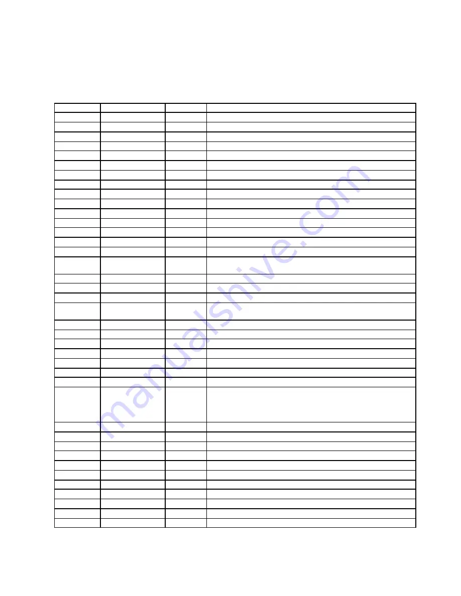
Pin No.
Terminal
In/Out
Function
1~7
D7~D0
I/O
Data bus.
11
GND7
In
Ground(0V) source.
12
CK16
Out
16.384MHz clock pulse output.
13
VCC6
In
+5V source
14
CK0
In
Clock pulse input. Connected to terinal CK16.
16
VCC1
In
+5V source.
17
GND1
In
Ground(0V) source.
18,19
XTI, XTO
In/Out
16.384MHz clock pulse input/output. Connected to crystal.
21
CCSB
I
Chip select signal input.
22~25
CA0~CA3
In
Address bus.
26
CE0
In
Connected to ground.(ROM interface ontrol terminal)
27
CWRB
In
Write enable signal.
28
CRDB
In
Read enebla signal.
33
RESB
In
Reset sna iput
34
TESB
In
Connected to +5V.
40~49
52~57
RD0~RD15
In
Data bus for sound source ROM.
50
VCC2
In
+5V source.
51
GND2
In
Ground(0V) source.
59
RA22
Out
Chip enable signal output for ROM.
62~73
75~82
RA0~RA19
Out
Address bus for sound source ROM.
74
GND5
In
Ground(0V) source.
84
VCC3
In +5V
source.
85
GND3
In
Ground source.
86
WOK1
Out
Ward clock for DAC.
88
SOLP
Out
16-bit serial data for L-channel DAC.
89
BOK
Out
Bit clock for DAC.
93
VCC5
In
+5V source.
95,97
99~105
107,109
110,112
EA0~EA12
Out
Address bus for RAM.
96
EWEB
Out
Write enable signal for RAM.
106
EOEB
Out
Read enable signal for RAM.
108
VCC7
In
+5V source.
111
ECEB
Out
Chip eneble signal for RAM.
118
VCC4
In
+5V source.
119
GND4
In
Ground(0V) source.
123~130
ED0~ED7
In/Out
Data bus for RAM.
131
GND6
In
Connected to Ground.
132
SSI
In
Connected to Ground.
133
SBCK
In
Connected to Ground.
134
SWCK
In
Connected to Ground.
Summary of Contents for CTK-650
Page 1: ...with price CTK 650 ELECTRONIC KEYBOARD R CTK 650...
Page 14: ...12 1 10 11 12 13 2 5 3 6 4 7 17 8 9 16 15 19 18 14 PCB VIEW MAJOR WAVEFORMS...
Page 15: ...13 18 19 16 17 9 8 14 15 4 7 3 6 2 5 10 11 12 13 1 SCHEMATIC DIAGRAM M5711 MA1M...
Page 16: ...14 SCHEMATIC DIAGRAM M5711 CN1M...
Page 21: ...19 EXPLODED VIEW...
Page 22: ...MA0200941A...