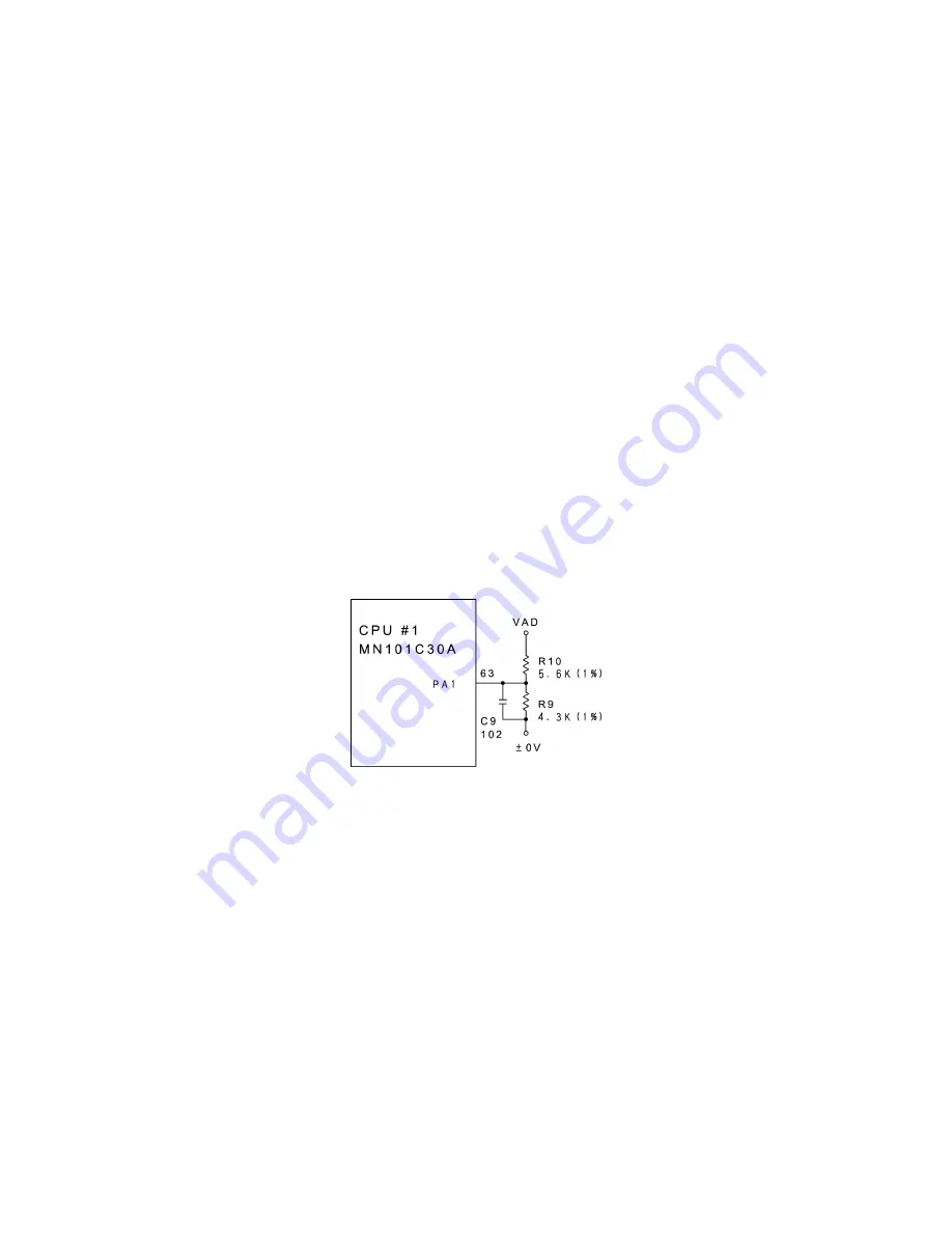
background image

III

 - 12

3.2.8

Voltage Detection Circuit

Figure 3.2-12 shows the voltage detection circuit which is composed of a resistor
network.

Voltage detection circuit

This circuit, which is composed of divider resistors R9 and R10, steps down the power
source VAD fed from dry cells or the AC adapter and feeds the output to the A/D input
port PA1 on the CPU.  According to the drive source voltage, the CPU determines the
optimum head drive power.

During non-printing:

If the voltage level of the VAD drops below approx. 6.8V, the CPU immediately shuts
down the power.

Ÿ

Adapters with an output of 10.8 V or greater are designated as "high-voltage" adapters
and cannot be used for this machine.  If this machine detects any high-voltage adapter
plugged in, it will power itself off.

During printing:

Ÿ

If it drops even more below approx. 5.7V, the CPU displays the "BATTERY" message
to warn you of a low battery after completion of printing.

Ÿ

If it drops below approx. 5.2V, the CPU immediately shuts down the power.


Figure 3.2-12  Voltage Detection Circuit

Summary of Contents for P-touch 65

Page 1: ...SERVICE MANUAL MODEL P touch 65 P touch HOME HOBBY P touch One ...

Page 2: ...SERVICE MANUAL MODEL P touch 65 P touch HOME HOBBY P touch One ...

Page 3: ...ht Brother 2000 All rights reserved No part of this publication may be reproduced in any form or by any means without permission in writing from the publisher Specifications are subject to change without notice ...

Page 4: ...persons to accurately and quickly provide after sale service for our P touch 65 P touch HOME HOBBY P touch One To perform appropriate maintenance so that the machine is always in best condition for the customer the service personnel must adequately understand and apply this manual This manual is made up of four chapters and appendices CHAPTER I SPECIFICATIONS CHAPTER II MECHANISMS CHAPTER III ELEC...

Page 5: ...Chapter I SPECIFICATIONS ...

Page 6: ... SPECIFICATIONS I 1 1 1 1 External Appearance I 1 1 1 2 Keyboard I 1 1 1 3 Display I 1 1 1 4 Printing Mechanism I 2 1 1 5 Tape Cassette I 2 1 1 6 Tape Cutter I 2 1 2 ELECTRONICS SPECIFICATIONS I 4 1 2 1 Character Generator I 4 1 2 2 Power Supply I 4 ...

Page 7: ...cassette 1 1 2 Keyboard 1 Entry system Rubber key pad 2 Number of alphanumeric and symbol keys 31 3 Number of function keys 12 including On Off key 4 Key arrangement See Figure 1 1 2 1 1 3 Display 1 Display type Liquid crystal display LCD 2 Number of columns 8 columns x 1 rows See Figure 1 1 2 3 Number of indicators 11 See Figure 1 1 2 4 Character size 5 dots wide by 7 dots high 5 Field of view an...

Page 8: ...haracter size dots Height x Width Standard Small size 1 32 x 20 Double width W2 32 x 40 Double height H2 64 x 20 Large size 4 64 x 40 1 1 5 Tape Cassette 1 Cassette Cartridge type 2 Tape type Direct thermal print tape Metal deposit layer on substrate 3 Tape size Width 9 12 mm Length 8 m 4 Tape cassette packed with the Character color Black machine Tape color White Tape width 12 mm or 9 mm EU Tape ...

Page 9: ...I 3 Figure 1 1 2 Key Arrangement ...

Page 10: ...ape cassette and then some at room temperature and normal humidity 4 Automatic powering off Yes If the machine remains unused for approx 5 minutes it automatically powers itself off 5 Low battery indication 1 If the voltage level drops below approx 5 7V the CPU displays the BATTERY message to warn you of low battery after completion of printing 2 If it drops further below approx 5 2V the CPU immed...

Page 11: ...Chapter II MECHANISMS ...

Page 12: ...Sub PCB Main PCB and Rubber Key Pad II 11 4 Taking out the and Terminal ASSYs 65 Terminals P1 and P3 and Battery Terminals P2 II 12 5 Unsoldering the and Terminal ASSYs 65 and Sub PCB Leads from the Main PCB II 14 2 2 2 Reassembly Procedure II 15 1 Soldering the Sub PCB Leads and and Terminal ASSYs 65 onto the Main PCB II 15 2 Setting the Battery Terminals P2 Terminals P3 and P1 and and Terminal A...

Page 13: ...ower to the selected ones of those 64 heating elements The selected heating element s generates heat that dissolves the metal deposit layer of the thermal tape so as to reveal the substrate layer producing a dot on the tape The tape is advanced and the next heating cycle is repeated thus forming a character on the tape n Character Formation While the drive motor DC motor feeds the tape by 0 106 mm...

Page 14: ...s pivots the roller holder ASSY around the shaft provided on the chassis so as to press the roller holder ASSY against the thermal head The platen is pressed perpendicularly against the thermal head with the tape sandwiched inbetween under a uniform load by the platen spring At the same time the platen gear becomes engaged with the drive gear of the gear train on the chassis see Figure 2 1 3 Openi...

Page 15: ...se the cassette cover the platen and the thermal head sandwich the tape inbetween and the platen gear becomes engaged with the gear train as described in Subsection 2 1 2 As the DC motor rotates the rotation is transmitted via the gear train to the platen gear Accordingly the sandwiched tape will be advanced Figure 2 1 3 Tape Feed Mechanism ...

Page 16: ...out the blade from the cutter unit to press the printed tape against the cutter board of the tape cassette cutting the printed tape coming through the cutter unit and the cutter board When the cassette cover is opened and no tape cassette is loaded the cutter safety mechanism works to lock the cutter lever as described in Subsection 2 1 5 Figure 2 1 4 Tape Cutter Mechanism ...

Page 17: ...for safety as shown below Closing the cassette cover or loading a tape cassette releases the cutter safety lock mechanism as follows Closing the cassette cover pivots the roller holder ASSY towards the thermal head so that the cutter lever stopper does not interfere with the cutter lever When a tape cassette is loaded its outer edge pushes the tab of the roller holder ASSY to pivot the roller hold...

Page 18: ...es PCBs and covers 4 Be careful not to lose screws washers or other parts removed for parts replacement 5 Tighten screws to the torque values listed below n n Tightening Torque List Location Screw type Q ty Tightening torque Bottom cover Taptite bind B M2 6 x 8 4 0 39 0 10 N m 4 1 kgf cm Chassis ASSY Taptite bind B M2 6 x 4 3 0 196 0 049 N m 2 0 5 kgf cm Chassis ASSY for motor Screw pan M1 7 x 2 5...

Page 19: ...ress section A of the cassette cover to release the latch and then remove the cassette cover Figure 2 2 1 Removing the Cassette Cover 3 Remove the six dry cells tape cassette and cutter unit For easier removal of the tap cassette lift up the front edge and then take it out Figure 2 2 2 Removing the Dry Cells Tape Cassette and Cutter Unit ...

Page 20: ...s ASSY 1 Remove the four screws from the bottom cover Figure 2 2 3 Unscrewing the Bottom Cover 2 Slightly open the bottom cover and disconnect the head flat cable from the main PCB Figure 2 2 4 Disconnecting the Head Flat Cable ...

Page 21: ...is ASSY The FG wire also comes off 4 Unsolder the motor lead wires from the main PCB Figure 2 2 5 Unsoldering the Motor Lead Wires and Removing the Chassis ASSY 5 Lift the chassis ASSY up and out of the bottom cover The cutter lever also comes off ...

Page 22: ...to the electricity charged in your body 1 Remove the screw from the thermal head ASSY and take off the ASSY 2 Remove the retaining ring from the shaft of the chassis ASSY 3 Pull up the roller holder ASSY together with the spring 4 Remove the two screws from the chassis ASSY and take off the DC motor ASSY Figure 2 2 6 Disassembling the Chassis ASSY ...

Page 23: ...e 2 2 7 Taking out the Sub PCB 2 Remove the two screws from the main PCB 3 Slightly slide the main PCB to the front press the latches provided on the body cover outwards and then take out the LCD by gently pulling out the main PCB and LCD flat cable 4 Take out the rubber key pad Figure 2 2 8 Taking out the Main PCB and Rubber Key Pad from the Body Cover ...

Page 24: ...iver and from the bottom push the terminal ASSY up and out of the bottom cover 2 In the same manner as in step 1 remove the terminals P1 and P3 3 Turn the bottom cover upside down unlatch the locking pawl of the terminal ASSY 65 with the flat screwdriver and push the terminal out of the bottom cover Figure 2 2 9 Taking out the and Terminal ASSYs 65 and Terminals P1 and P3 ...

Page 25: ...II 13 4 As shown below press the locking pawl of each battery terminal P2 with a flat screwdriver and push it out from the bottom cover Figure 2 2 10 Taking out the Battery Terminals P2 ...

Page 26: ...cessary to separate the and terminal ASSY 65 or sub PCB leads from the main PCB unsolder them with a soldering iron 1 Unsolder the and terminal ASSYs 65 from the main PCB 2 European version To remove the sub PCB unsolder the four lead wires from the main PCB Figure 2 2 11 Unsoldering the and Terminal ASSYs 65 and Sub PCB Leads ...

Page 27: ...he European version 1 European version Solder the four lead wires of the sub PCB to the main PCB according to the wire ID colors as shown below 2 Solder the and terminal ASSYs 65 according to the wire ID colors as shown below Figure 2 2 12 Soldering the Sub PCB Leads and the and Terminal ASSYs 65 European version US version ...

Page 28: ... the bottom cover until they snap into place as shown below Figure 2 2 13 Setting the Battery Terminals P2 3 Turn the bottom cover rightside up 4 Snap the terminal ASSY 65 into the bottom cover 5 Snap the terminals P3 and P1 into the bottom cover 6 Snap the terminal ASSY 65 into place Figure 2 2 14 Setting the Terminals P3 and P1 and the and Terminal ASSYs 65 ...

Page 29: ...e is no foreign material or dust on the key contacts of the main PCB 3 While pressing the latches on the body cover outwards slide the LCD as illustrated below Make sure that the LCD is fully fitted in the body cover 4 Secure the main PCB to the body cover with two screws Figure 2 2 15 Reinstalling the Rubber Key Pad and Main PCB 5 European version Secure the sub PCB with two screws Figure 2 2 16 ...

Page 30: ...ack into the bottom cover 4 Secure the chassis ASSY with three screws One of those screws should also secure the FG wire NOTE Check that the FG wire is secured to the correct position referring to the illustration given below 5 Solder the motor lead wires to the main PCB as shown below NOTE Check the wire ID colors then solder the black and red wires to the and points respectively Figure 2 2 17 In...

Page 31: ...e head flat cable to the main PCB and close the bottom cover Figure 2 2 18 Routing the and Terminal ASSYs 65 and Connecting the Head Flat Cable 8 Secure the bottom cover to the body cover with four screws taking care not to pinch the wires between the body cover and bottom cover Figure 2 2 19 Securing the Bottom Cover to the Body Cover ...

Page 32: ...roller holder ASSY so that its straight end is fitted into section A on the ASSY then install them to the chassis and secure the ASSY with the retaining ring 3 As shown below turn the bent end of the roller holder spring with a flat screwdriver and fit it into an oval hole provided in the chassis Then secure the thermal head ASSY with a screw Figure 2 2 20 Assembling the Components of the Chassis ...

Page 33: ...y Cells and Cassette Cover 1 Set the cutter unit into place 2 Set a tape cassette 3 Load dry cells 4 Fit hooks X of the cassette cover and then snap the cover into place Figure 2 2 21 Setting the Cutter Unit Tape Cassette Dry Cells and Cassette Cover ...

Page 34: ...ralian versions operates correctly 9 Replace the dry cells with new ones and then power on the machine 10 Check the tape feeding length according to the steps below 1 While holding down the Code key press the Space key to feed tape 2 Push the cutter lever to cut the tape 3 Enter arbitrary characters 4 While holding down the Code key press the H key After the print preview the tape length will appe...

Page 35: ...Chapter III ELECTRONICS ...

Page 36: ...III 4 1 Key contacts matrix III 4 2 Solder points III 6 3 2 5 Power ON OFF Key and Reset Circuit III 7 1 Power ON OFF circuit III 7 2 Automatic powering off circuit III 8 3 2 6 Motor Drive Circuit III 9 3 2 7 Thermal Head Drive Circuit III 10 3 2 8 Voltage Detection Circuit III 12 3 2 9 Oscillation Circuit III 13 3 2 10 Power Supply Circuit III 14 3 3 SUB PCB III 15 3 3 1 Sub PCB III 15 ...

Page 37: ... print head n Motor The DC motor is a power source to advance tape It operates on 9V unstabilized n Thermal Print Head This is a thick film thermal print head which integrates a heat generator consisting of 64 heating elements vertically aligned and driver circuitry When selectively energized by 9V unstabilized those heating elements produce characters n LCD The LCD is 8 characters wide by one row...

Page 38: ... CPU including a ROM and RAM 2 LCD controller 3 Key contacts matrix and solder points destination switching circuit 4 Power ON OFF circuit 5 Motor drive circuit 6 Thermal head drive circuit 7 Voltage detection circuit 8 Oscillation circuit 9 Power supply circuit Provided for the European version Figure 3 2 1 Main PCB Block Diagram ...

Page 39: ...an 8 bit microprocessor produced by CMOS silicon gate process which integrates a 32 kilobyte ROM and a 1 5 kilobyte RAM 3 2 3 LCD Controller LCDC 3 SPLC 780A2 drives the LCD in 1 8 duty and 1 4 bias levels Figure 3 2 2 CPU and LCD Controller ...

Page 40: ... carbon printed on the main PCB Figure 3 2 4 shows a key scan timing scheme and scanning pulse outputs Ports P70 through P75 on the CPU issue a group of key scanning pulses Every scanning pulse is Low active for 200 µs and is in high impedance while inactive Ports P60 through P67 act as input ports which receive key status The CPU scans the key contacts matrix every 10 ms If the CPU reads the same...

Page 41: ...III 5 Figure 3 2 4 Key Scan Timing Scheme and Scanning Pulse Outputs ...

Page 42: ...er points A and C are reserved for the future use for the thermal head ranking The CPU reads the solder point status once in the powering on sequence to recognize the customization Figure 3 2 5 Keyboard and Solder Points 20 U S A Canada H H H 10 Germany H H H 02 Belgium H L H 01 France L H H 00 England H H H Spec No Destination 1 2 3 Solder Points H Solder point opened L Solder point closed ...

Page 43: ...ferent from other keys although the ON OFF key is on the same key pad Figure 3 2 6 ON OFF Key The ON OFF key is held down during which the CPU is inactive ƒ Reset operation by the reset circuit ƒ In the powering on sequence The reset signal is canceled and the program starts ƒ In the powering off sequence The reset signal is canceled and the program stops Figure 3 2 7 Powering on off sequence ...

Page 44: ...t If you power off the machine with the ON OFF key or you make no key entry for approx 5 minutes the oscillation stops so that the CPU enters the sleep mode To cancel the sleep mode and resume the normal operation mode press the ON OFF key ...

Page 45: ...PU produces a start stop control signal to the motor drive circuit Figure 3 2 9 shows the part of motor waveforms 2 BA6220 is an electronic governor IC and controls to keep the rotation speed of the motor constant even if the power source voltage VBT varies Figure 3 2 8 Motor Drive Circuit Figure 3 2 9 Part of Motor Waveforms ...

Page 46: ...drivers the heating elements of the thermal head according to the signal issued from P03 Figure 3 2 11 illustrates a timing chart of the thermal head drive Capacitor C10 works as a thermal head overheat protector It cuts off the P03 signal to shut down invalid drive current if the signal sticks to the low level due to any malfunctions of the programs or the CPU Since thermal heads are very sensiti...

Page 47: ...III 11 Figure 3 2 11 Timing Chart for Thermal Head Drive ...

Page 48: ...mum head drive power During non printing If the voltage level of the VAD drops below approx 6 8V the CPU immediately shuts down the power Ÿ Adapters with an output of 10 8 V or greater are designated as high voltage adapters and cannot be used for this machine If this machine detects any high voltage adapter plugged in it will power itself off During printing Ÿ If it drops even more below approx 5...

Page 49: ...2 13 shows the oscillation circuit This circuit contains an oscillator and generates 8 MHz frequency which acts as the CPU basic clock The CPU divides this into half 4 MHz to synchronize its internal operations Figure 3 2 13 Oscillation Circuit ...

Page 50: ... 2 10 Power Supply Circuit Figure 3 2 14 shows the power supply circuit The 3 terminal regulator RH5RL50A stabilizes the battery output producing the 5BV power source 5 0 125V Figure 3 2 14 Power Supply Circuit ...

Page 51: ...III 15 3 3 SUB PCB 3 3 1 Sub PCB The sub PCB is provided for the European version and allows you to connect an AC adapter Figure 3 3 1 Sub PCB Circuit ...

Page 52: ...Chapter IV TROUBLESHOOTING ...

Page 53: ...NG IV 1 4 1 1 Precautions IV 1 4 1 2 After Repairing IV 1 4 1 3 Troubleshooting Flows IV 2 1 Tape feeding failure IV 2 2 Printing failure IV 5 3 Powering failure Nothing appears on the LCD IV 8 4 No key entry possible IV 10 5 Abnormal LCD indication IV 11 ...

Page 54: ...rouble is Whenever more than one trouble source is found plan the most reasonable repairing procedure after reviewing the relationship between them 2 When supplying power to this machine having problems with either a set of batteries or the AC line adapter make sure that its output voltage level is 8 to 10V under no load 3 When using a circuit tester for testing the conductivity remove all of the ...

Page 55: ...IV 2 4 1 3 Troubleshooting Flows 1 Tape feeding failure ...

Page 56: ...IV 3 ...

Page 57: ...IV 4 ...

Page 58: ...IV 5 2 Printing failure ...

Page 59: ...IV 6 ...

Page 60: ...IV 7 ...

Page 61: ...IV 8 3 Powering failure Nothing appears on the LCD ...

Page 62: ...IV 9 ...

Page 63: ...IV 10 4 No key entry possible ...

Page 64: ...IV 11 5 Abnormal LCD indication ...

Page 65: ...APPENDICES Circuit Diagrams A Main PCB B Sub PCB for P touch 65 and P touch One only ...

Page 66: ...S E G 3 1 S E G 2 8 S E G 2 7 S E G 2 6 S E G 1 9 S E G 1 8 S E G 1 7 S E G 1 6 S E G 1 5 S E G 1 4 S E G 1 3 S E G 1 2 S E G 1 1 S E G 1 0 S E G 9 S E G 8 S E G 7 S E G 6 S E G 5 S E G 4 S E G 4 0 S E G 3 0 S E G 2 9 S E G 2 5 S E G 2 4 S E G 2 3 S E G 2 2 S E G 2 1 S E G 2 0 S E G 3 S E G 2 S E G 1 S E G 9 S E G 1 4 S E G 4 0 S E G 3 9 S E G 3 8 S E G 3 7 S E G 3 6 S E G 3 5 S E G 3 4 S E G 2 5 ...

Page 67: ...D C J A C K V B T 0 V A C S E N S C 1 1 0 4 H E C 0 4 7 1 0 1 6 3 0 3 R 0 A 3 R 0 R 8 C E R B 8 3 0 0 4 1 S S 1 3 3 R 1 NAME CODE LA3766000 SUB PCB CIRCUIT DIAGRAM PT65 Appendix B Sub PCB ...

Page 68: ...May 2000 8V2008BE0 Printed in Japan ...

Reviews: