I-6
3.
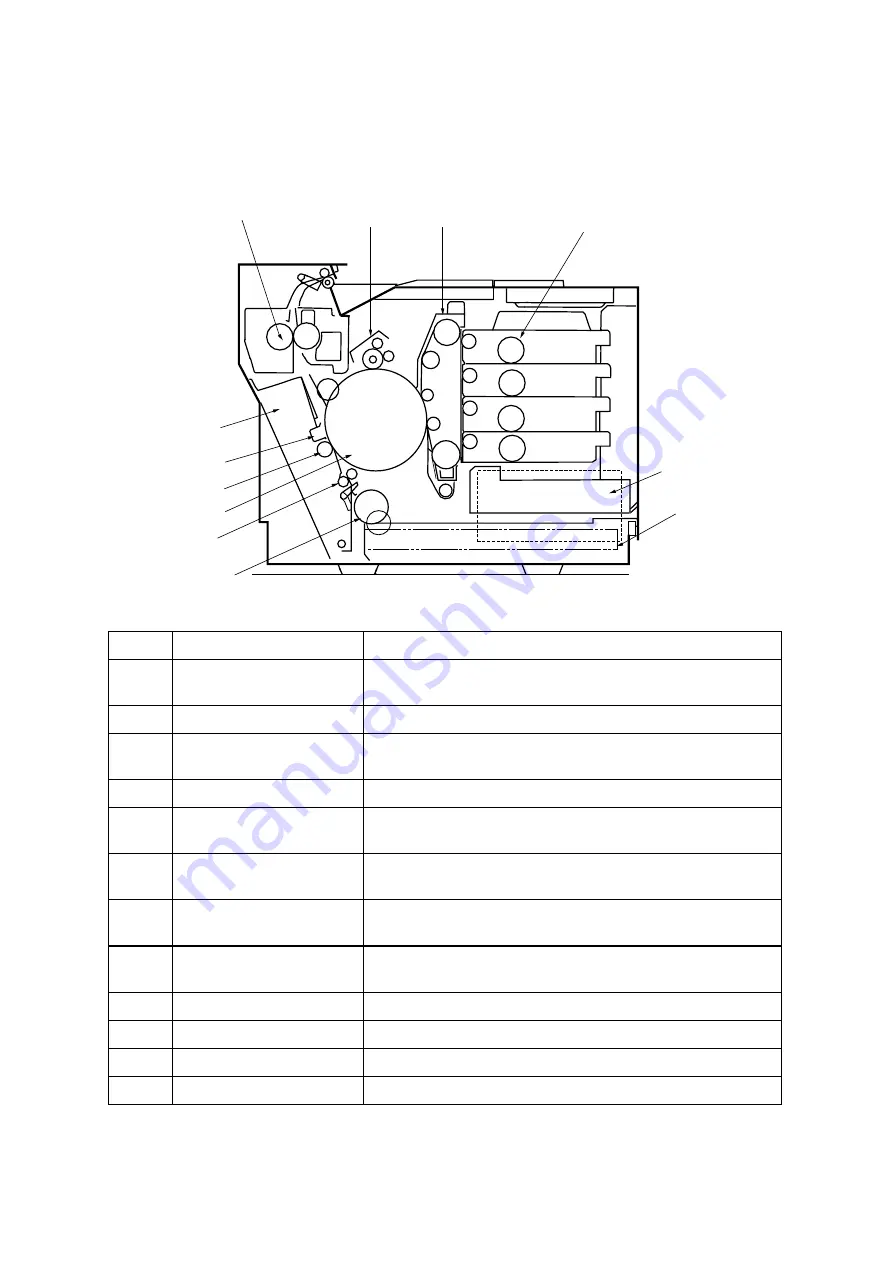
INTERNAL STRUCTURE
<Cross Sectional View >
K
Y
M
C
Fig.1-3
No.
Components Name
Outline of Functions
1 Toner
Cartridge
Contain the toner (K, Y, M, C) for developing.
Each toner cartridge (K, Y, M, C) is independent.
2
OPC Belt Cartridge
Forms images and includes the photoconductive belt.
3
Drum Cleaner 2
Cleans and collects waste toner adhering to the transfer
drum 2.
4
Fusing Unit
Fixes by heat and pressure the toner image onto the paper.
5
Transfer unit 2
Transfers toner images from the transfer drum 2 to the
paper.
6
Transfer Drum 2
Forms color images, combining the toner images from the
OPC belt on the drum.
7 Paper
Discharger
Emits a corona charge for separating the paper from the
transfer drum 2.
8
Transfer Roller 2
Transfer the toner image on the transfer drum 2 to the
paper.
9
Media Cassette
Feeds paper automatically.
10
Paper Pick-up Roller
Feeds paper automatically from the paper cassette.
11
Scanner Unit
Generates a laser beam and scans the OPC belt.
12
Registration Roller 2
Aligns the paper correctly ready for printing
4.Fusing Unit
3.Drum Cleaner 2
2.OPC Belt Cartridge
8.Transfer Roller 2
9.Media Cassette
11.Scanner Unit
1.Toner Cartridge (K, Y, M, C)
10.Paper Pick-up Roller
12.Registration Roller 2
6.Transfer Drum 2
7.Paper Discharger
5.Transfer Unit 2
Summary of Contents for HL-2600CN Series
Page 14: ...viii 3 Rating Label For US For Europe Jam label ...
Page 16: ... 37 5 352 8 7 287 1 ...
Page 26: ...CHAPTER II SPECIFICATIONS ...
Page 38: ... 37 5 167 7 21 ...
Page 50: ...CHAPTER IV STRUCTURE OF SYSTEM COMPONENTS ...
Page 99: ...Main PCB Circuit Diagram 1 8 CODE B512137CIR 1 8 LJ8907001 IV 48 NAME ...
Page 100: ...Main PCB Circuit Diagram 2 8 CODE B512137CIR 2 8 LJ8907001 IV 49 NAME ...
Page 101: ...Main PCB Circuit Diagram 3 8 CODE B512137CIR 3 8 LJ8907001 IV 50 NAME ...
Page 102: ...Main PCB Circuit Diagram 4 8 CODE B512137CIR 4 8 LJ8907001 IV 51 NAME ...
Page 103: ...Main PCB Circuit Diagram 5 8 CODE B512137CIR 5 8 LJ8907001 IV 52 NAME ...
Page 104: ...Main PCB Circuit Diagram 6 8 CODE B512137CIR 6 8 LJ8907001 IV 53 NAME ...
Page 105: ...Main PCB Circuit Diagram 7 8 CODE B512137CIR 7 8 LJ8907001 IV 54 NAME ...
Page 106: ...Main PCB Circuit Diagram 8 8 CODE B512137CIR 8 8 LJ8907001 IV 55 NAME ...
Page 108: ...IV 57 Layout of Connector Pin Assignment Power Supply Unit Fig 4 40 ...
Page 112: ...IV 61 Layout of Connector Pin Assignment High Voltage Power Supply Unit Fig 4 41 ...
Page 124: ...CHAPTER V CONTROL PANEL OPERATION ...
Page 170: ...CHAPTER VI 3 5 2 0 17 1 1 ...
Page 210: ...CHAPTER VII 6 66 0 ...
Page 286: ... 37 5 9 7528 6 227 1 ...
Page 330: ...9 5 IMAGE FAILURE 1 2 3 4 5 6 7 8 9 a 9 b 10 11 12 13 14 ...
Page 331: ...9 15 a 15 b 16 17 18 19 20 21 22 23 24 25 26 27 28 Fig 8 2 ...
Page 351: ...A 4 6 Transfer Drum Hand writing X X X X X X 7 1 2 3 Location DATE MONTH SERIAL NO YEAR ...
Page 366: ...A 19 6 Fix the four joints then band the box with two plastic bands P P band Joint ...


