AUREL 650201515G User Manual Download Page 32


             RTX-24EM-HP


User guide  


The technical characteristics can change without notice. AUR°EL S.p.A doesn’t assume the responsibility to the damages caused by an improper use of the  device. 
 

AUR°EL S.p.A.

 Via Foro dei Tigli, 4 - 47015 Modigliana (FC) – ITALY                                                                 12/11/2019 - Rev. A  

Tel.: +390546941124 – Fax: +390546941660                                                                                                                   Page  32 

http://www.aurel.it


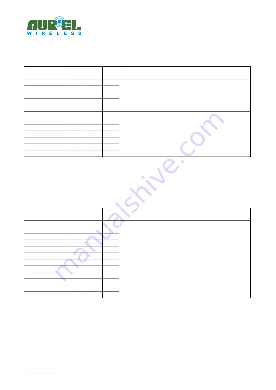
RAM2[11:0]@ Address 6 


Bit 

Default 

Value 

Reset 
Value 

Description 

I_PA[4] 

11 

Current bias of the PA. Defines RF output in Transmit mode. 

I_PA[3] 

10 

I_PA[2] 

I_PA[1] 

I_PA[0] 

Reserved 

Reserved. 

Reserved 

Reserved 

Reserved 

Reserved 

Reserved 

Reserved 


RAM2[11:0]@ Address 7 


Bit 

Default 
Value 

Reset 
Value 

Description 

Reserved 

11 

Reserved. 

Reserved 

10 

Reserved 

Reserved 

Reserved 

Reserved 

Reserved 

Reserved 

Reserved 

Reserved 

Reserved 

Reserved 


Summary of Contents for 650201515G

Page 1: ...onditions 6 2 Supply currents on Vcc 6 3 RF characteristics 7 Functional modes 7 1 Power Down 7 2 Standby Mode 7 3 RAM2 Init 7 4 Auto cal 7 5 Transmit 7 6 Receive 8 Digital interface 8 1 SPI operation...

Page 2: ...ing 21 9 6 RF operating frequency 22 9 7 Address byte 22 9 8 TX Power level 23 9 9 Packet TX and RX payload 23 9 9 1 Mode payload size in the header 23 9 9 2 Mode payload size in RAM2 23 9 10 Register...

Page 3: ...e provides a simple control of the baseband using an external host microcontroller The EM9209 provides two communication modes with normal sensitivity NS or high sensitivity HS and programmable bit ra...

Page 4: ...er tive low from the external host microcontroller to the radio module forced to low level the device is resetted and in power down mode Master Out Slave In SPI signal from the external host microcont...

Page 5: ...ource protected against short circuits The usage of the transceiver is foreseen inside enclosures that assure the overcoming of the rule EN 61000 4 2 not directly applicable to the module itself This...

Page 6: ...elow 5 1 1 Frequency synthesizer Phase Locked Loop PLL The frequency synthesizer provides an accurate low jitter 100 dBc 1MHz offset 2 4GHz RF signal used for both up conversion in Transmit mode and d...

Page 7: ...configuration ontroller drives an interrupt pin IRQ which can be programmed to indicate the status that a packet has been sent or received or that auto calibration has finished This controller to comp...

Page 8: ...5 2 1 2 In Auto calibration mode The center frequency of the VCO is tuned for a chosen channel frequency The result of the auto calibration is directly written in the VCO center frequency register VCO...

Page 9: ...ts on Vcc Operating Mode Notes Symbol Conditions Min Typ Max Unit Power Down ICC_PWDOWN ENABLE Pin 10 or nRESET Pin 4 0 2 A Standby ICC_STDBY ENABLE Pin 10 or nRESET Pin 4 1 and 26MHz crystal oscillat...

Page 10: ...cing FCHW 4 MHz Transmitter Operation RF Output power on UFL connector RTX 24EM HP AE H and RTX 24EM HP AE V versions See note 4 3 4 PRFMAX 20 dBm See note 4 3 4 PRFEU 10 dBm E R P RF power RTX 24EM H...

Page 11: ...sibility to the damages caused by an improper us 47015 Modigliana FC ITALY Fax 390546941660 operational modes of the RTX 24EM HP module An example state diagram is described below The SPI interface is...

Page 12: ...bration mode that must be run periodically by the host microcontroller This keeps the channel frequency and FSK modulator operating within specification Analog components in this block are sensitive t...

Page 13: ...ata in to RTX 24EM HP MISO Serial data out of RTX 24EM HP The RTX 24EM HP has a programmable interrupt pin IRQ All internal enables signals and parameters of the RTX 24EM HP are mapped in a small 16x1...

Page 14: ...to MOSI hold 20 ns tSD SS to MISO Valid 30 ns tCD SCK to MISO Valid 30 ns tSCKL SCK low time 40 ns tSCKH SCK high time 40 ns fsck SCK frequency 0 10 MHz tCS SS to SCK Setup 20 ns tCH SCK to SS Hold 2...

Page 15: ...operation works together with the internal microcontroller and is functional only when this latter has been started SPI command Start_Micro and when the master clock is active Crystal oscillator must...

Page 16: ...ead_RAM1 This command reads the 12 bits word from the specified address 6bits of RAM1 This command will put the microcontroller on hold and reset state until last bit has been processed Write_RAM1 Thi...

Page 17: ...nd FIFO s content could be corrupted Always first stop the micro using SPI command Stop_Micro prior to use Reset_Micro Stop_Micro This command stops the microcontroller Start_Micro This command start...

Page 18: ...om the specified ROM address to RAM1 This allows for fast initialization of the microcontroller subroutines The crystal oscillator must be enabled to perform this operation Additionally ROM_Boot comma...

Page 19: ...ivity can be monitored through Status 1 by using a simple Stop_Micro SPI command for example When Status 1 has gone low the RAM2 initialization subroutine can be executed Use SPI command Write_RAM1 wi...

Page 20: ...has a dedicated subroutine located at the ROM_Boot_Address 64 which will perform the VCO auto calibration Auto calibration frequency is set through register VcoCalibFreq 11 0 which is located in RAM1...

Page 21: ...rates are available Ch_Rate 2 0 000 to 011 On air bit rate kbps Ch_Rate 2 0 R_Bit_Clk 8 0 RAM2 12 11 0 1 5 000 110000000 0x180 2 99 001 011000000 0x2C0 6 02 010 001011111 0x45F 12 037 011 000101111 0...

Page 22: ...he same channel The host microcontroller can program a channel change which is validated when SPI signal SS goes down Channel spacing of 4 MHz is recommended to limit interference with other RTX 24EM...

Page 23: ...antenna has a 0dB maximum gain Note 2 the European standard EN 300 440 allows maximum 10dBm RF radiated power This means that with this power setting the device with integrated antenna is not in compl...

Page 24: ...Micro will reset all internal TXFIFO and RXFIFO pointers to 0 9 11 Received Signal Strength Indicator RSSI A received signal strength indicator RSSI is available through the register Limit_RSSI 3 0 lo...

Page 25: ...4 Send the SPI command ROM_Boot with ROM_Boot_Address 0 to perform the RAM2 initialization 5 Send the SPI command Write_RAM1 with address 13 and data write 1184 to set RB_Inst_Dis 1 6 Send the SPI co...

Page 26: ...on mode In this case the next packet transmission requires to execute only steps 24 to 27 Note 1 Transmission mode is started from reception mode So it is not possible to exclude that an incoming pack...

Page 27: ...dress 33 to perform the PTAT auto calibration 9 Send the SPI command Start_Micro 10 Wait the IRQ pin to go to high this will mean that the PTAT auto calibration subroutine has been executed 11 Clear I...

Page 28: ...frequency is close to channel data rate correct reception operation can be corrupted SPI commands to retrieve RAM2 values such as Limit_RSSI 3 0 or DFT_Mes 7 0 should be sent immediately after IRQ si...

Page 29: ...Value Description VDD_Synth_En 11 1 0 VDD_Synth Voltage Regulator enable VDD_RXTX_En 10 1 0 VDD_RXTX Voltage Regulator enable Xtal_En 9 1 0 Crystal oscillator enable Reserved 8 1 0 Reserved Reserved...

Page 30: ...Reset Value Description Reserved 11 1 0 Reserved Reserved 10 0 0 Reserved 9 1 0 Reserved 8 0 0 Reserved 7 0 0 Reserved 6 0 0 Reserved 5 0 0 Reserved 4 1 0 Reserved 3 0 0 Reserved 2 1 0 Reserved 1 0 0...

Page 31: ...re_PA 4 11 0 0 Current bias of the PA preamplifier Defines RF output power in Transmit mode I_Pre_PA 3 10 1 0 I_Pre_PA 2 9 1 0 I_Pre_PA 1 8 0 0 I_Pre_PA 0 7 1 0 Reserved 6 0 0 Reserved Reserved 5 0 0...

Page 32: ...6 Bit Default Value Reset Value Description I_PA 4 11 0 0 Current bias of the PA Defines RF output in Transmit mode I_PA 3 10 1 0 I_PA 2 9 0 0 I_PA 1 8 1 0 I_PA 0 7 1 0 Reserved 6 0 0 Reserved Reserve...

Page 33: ...n Reserved 11 0 0 Reserved Reserved 10 1 0 Reserved 9 0 0 Reserved 8 0 0 Reserved 7 1 0 Reserved 6 0 0 RB_Inst_Dis 5 0 0 ROMboot Instruction Disable Reserved 4 0 0 Reserved Limit_RSSI 3 3 0 0 RSSI val...

Page 34: ...l it RAM2 11 0 Address 10 Bit Default Value Reset Value Description Reserved 11 0 0 Reserved Reserved 10 0 0 Reserved 9 1 0 Reserved 8 0 0 Reserved 7 1 0 Reserved 6 0 0 Reserved 5 0 0 Reserved 4 0 0 R...

Page 35: ...Description Ch_Rate 2 11 0 0 Bandwidth of the normal sensitivity demodulator Ch_Rate 1 10 0 0 Ch_Rate 0 9 0 0 R_Bit_Ck 8 8 1 0 CODEC Bit clock frequency R_Bit_Ck 7 7 1 0 R_Bit_Ck 6 6 0 0 R_Bit_Ck 5 5...

Page 36: ...Value Reset Value Description Reserved 11 0 0 Reserved Reserved 10 0 0 Frequ 4 9 0 0 Synthesizer s RF Frequency LSB s Frequ 3 8 1 0 Frequ 2 7 1 0 Frequ 1 6 1 0 Frequ 0 5 0 0 N_Pay 4 4 0 0 Payload size...

Page 37: ...5 LSB s of the header represent the payload size of the packet for payload size defined in header mode ROM_Boot_Address 320 For payload size defined in RAM2 mode ROM_Boot_Address 192 the header is no...

Page 38: ...In order to obtain the performances described in the technical specifications and to comply with the operating conditions which characterize the certification the device must be mounted on a printed...

Reviews: