background image


MAX1000 User Guide 


www.arrow.com 


Page | 14 

July 2017 

3.3.4


SDRAM Memory 
 

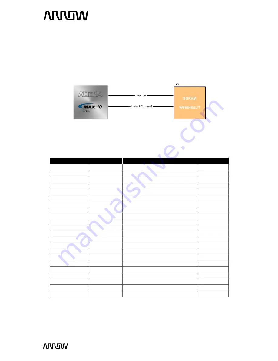
The MAX1000 board supports 64 MBit (default version) or up to 256 MBit (customized version) 
SDRAM which can operate up to 166 MHz clock frequency. Below are the connections and pinning 
of the SDRAM used in the MAX1000. 


Board Reference 

FPGA Pin No. 

Description 

I/O Standard 

A0 

PIN_K6 

SDRAM Address [0] 

3.3 V  

A1 

PIN_M5 

SDRAM Address [1] 

3.3 V  

A2 

PIN_N5 

SDRAM Address [2] 

3.3 V  

A3 

PIN_J8 

SDRAM Address [3] 

3.3 V  

A4 

PIN_N10 

SDRAM Address [4] 

3.3 V  

A5 

PIN_M11 

SDRAM Address [5] 

3.3 V  

A6 

PIN_N9 

SDRAM Address [6] 

3.3 V  

A7 

PIN_L10 

SDRAM Address [7] 

3.3 V  

A8 

PIN_M13 

SDRAM Address [8] 

3.3 V  

A9 

PIN_N8 

SDRAM Address [9] 

3.3 V  

A10 

PIN_N4 

SDRAM Address [10] 

3.3 V  

A11 

PIN_M10 

SDRAM Address [11] 

3.3 V  

A12 

PIN_L11 

SDRAM Address [12] 

3.3 V 

A13 

PIN_M12 

SDRAM Address [13] 

3.3 V  

BA0 

PIN_N6 

SDRAM Bank Address [0] 

3.3 V  

BA1 

PIN_K8 

SDRAM Bank Address [1] 

3.3 V  

CLK 

PIN_M9 

SDRAM Input Clock 

3.3 V  

CKE 

PIN_M8 

SDRAM Clock Enable 

3.3 V  

RAS 

PIN_M7 

SDRAM Row Address Strobe  

3.3 V  

CAS 

PIN_N7 

SDRAM Column Address Strobe  

3.3 V  

WE 

PIN_K7 

SDRAM Write Enable  

3.3 V  

CS 

PIN_M4 

SDRAM Chip Select  

3.3 V  


Figure 9 – SDRAM Connections


Summary of Contents for MAX1000

Page 1: ...MAX1000 User Guide Please read the legal disclaimer at the end of this document Revision 1 0 ...

Page 2: ...r 13 3 3 4 SDRAM Memory 14 3 3 5 Flash Memory 15 3 3 6 User I O 16 3 3 7 Arduino MKR Connectors 16 3 3 8 PMOD Connector 18 3 3 9 Communication and Configuration 19 3 3 10 Power Tree 21 Software and Driver Installation 22 4 1 Installing Quartus Prime Software Windows 22 4 2 Installing Arrow USB Programmer2 Windows 24 4 3 Installing Quartus Prime Software Linux 26 4 4 Installing Arrow USB Programmer...

Page 3: ...5 2 8 Connecting the Components 49 5 2 9 Analysis and Synthesis 55 5 2 10 Adding Timing Constraints 55 5 2 11 Pinning Assignments 58 5 2 12 Compiling the Design 61 5 2 13 Reading the Compilation Report 63 Configuring the MAX1000 64 6 1 Configure the FPGA in JTAG Mode 64 6 2 Internal Configuration 69 Common Issues and Fixes 71 Appendix 72 7 1 Revision History 72 7 2 Legal Disclaimer 73 ...

Page 4: ... 10 Figure 5 LED Connections 11 Figure 6 Button Debouncing 12 Figure 7 Button Connections 12 Figure 8 Accelerometer Connections 13 Figure 9 SDRAM Connections 14 Figure 10 Flash Connections 15 Figure 11 User I O Connections 16 Figure 12 Arduino MKR Header Connections 16 Figure 13 PMOD Header Connections 18 Figure 14 UART Connections 19 Figure 15 JTAG Connections 20 Figure 16 Power Tree Connections ...

Page 5: ...viding internally stored dual images with self configuration comprehensive design protection features integrated ADCs and hardware to implement the Nios II 32 bit microcontroller IP MAX10 devices are ideal solution for system management protocol bridging communication control planes industrial automotive and consumer applications The MAX1000 is equipped with an Arrow USB Programmer2 SDRAM flash me...

Page 6: ...MAX1000 or the MAX10 FPGA MAX1000 at Arrow Shop MAX1000 at Trenz Electronic Shop Intel MAX10 Webpage MAX1000 Wiki Page 1 3 GettingHelp Here are the addresses where you can get help if you encounter any problems Arrow Electronics In Person Arrow EMEA 49 0 6102 5030 0 Online https arrow com Trenz Electronic GmbH https www trenz electronic de en ...

Page 7: ...wing are available on the MAX1000 board Intel MAX 10 10M08SAU169C8G device Arrow USB Programmer2 on board for programming JTAG Mode 64MBit SDRAM 16 bit data bus 64Mbit Flash Memory One 12MHz MEMS Oscillator One optional MEMS Oscillator of preferred frequency Eight red user LEDs Two board indication LEDs Two user buttons One 3 axis accelerometer One 12 pin PMOD header One Arduino MKR header One Use...

Page 8: ...nt any system design FPGADevice Available MAX10 Devices for the MAX1000 Resources Device 10M02 10M04 10M08 10M16 Logic Elements LE K 2 4 8 16 M9K Memory K 108 189 378 549 User Flash K 96 1248 1376 2368 Internal Configuration Image 1 2 2 2 ADC 1 1 1 PLLs 2 2 2 4 ConfigurationandDebug On board Arrow USB Programmer2 mini USB type B connector MemoryDevices 64MBit to 128 MBit external flash memory 64MB...

Page 9: ...uino MKR Header User JTAG Header User I O Header ButtonsandIndicators 2 x side buttons 8 x red user LEDs 2 x board indication LEDs Sensors One 3 axis accelerometer Power Recommended external supply voltage range 5 0 V nominal Recommended I O signal voltage range 0 0 to 3 3 V ...

Page 10: ... the external clocks of the system can be seen in Figure 4 The default clock CLK12M is at 12 MHz and is connected and driving the FPGA s user logic and the Arrow USB Programmer2 There is an optional slot of another clock CLK_X to add another preferred clock source to the FPGA Both clocks are driving PLL1 PLL3 which are able to drive the ADC clock For more information on clocks and PLLs of the MAX1...

Page 11: ...A Each LED is driven directly and individually by the MAX10 FPGA driving its associated pin to a high logic level for on or low logic level for off Board Reference FPGA Pin No I O Standard LED1 PIN_A8 3 3 V LED2 PIN_A9 3 3 V LED3 PIN_A11 3 3 V LED4 PIN_A10 3 3 V LED5 PIN_B10 3 3 V LED6 PIN_C9 3 3 V LED7 PIN_C10 3 3 V LED8 PIN_D8 3 3 V Figure 5 LED Connections ...

Page 12: ...nput signal for improved noise immunity especially for signal with slow edge rate and acts as switch debouncer Push buttons drive their associated pins low logic level when pressed and high logic level when released Board Reference FPGA Pin No Description I O Standard RESET PIN_E7 Dual function Pin GPIO or nCONFIG 3 3 V Schmitt Triger USER_BTN PIN_E6 User button 3 3 V Schmitt Triger Figure 6 Butto...

Page 13: ... 16g and it is capable of measuring accelerations with output data rates from 1 Hz to 5 kHz The supplied power to the board coming either from micro USB connection or user Vin can be monitored through the ADC channel 3 of the accelerometer Board Reference FPGA Pin No Description I O Standard SEN_INT1 PIN_J5 Interrupt 1 3 3 V SEN_INT2 PIN_L4 Interrupt 2 3 3 V SEN_SDI PIN_J7 Data In MOSI 3 3 V SEN_S...

Page 14: ...A4 PIN_N10 SDRAM Address 4 3 3 V A5 PIN_M11 SDRAM Address 5 3 3 V A6 PIN_N9 SDRAM Address 6 3 3 V A7 PIN_L10 SDRAM Address 7 3 3 V A8 PIN_M13 SDRAM Address 8 3 3 V A9 PIN_N8 SDRAM Address 9 3 3 V A10 PIN_N4 SDRAM Address 10 3 3 V A11 PIN_M10 SDRAM Address 11 3 3 V A12 PIN_L11 SDRAM Address 12 3 3 V A13 PIN_M12 SDRAM Address 13 3 3 V BA0 PIN_N6 SDRAM Bank Address 0 3 3 V BA1 PIN_K8 SDRAM Bank Addre...

Page 15: ...ta 14 3 3 V DQ15 PIN_A12 SDRAM Data 15 3 3 V DQM0 PIN_E9 SDRAM Lower Data Mask 3 3 V DQM1 PIN_F12 SDRAM Upper Data Mask 3 3 V 3 3 5 FlashMemory The MAX1000 board supports up to 128 MBit of serial flash memory that can be used for user data and programming non volatile storage Single SPI interface is supported that can reach up to 104 MHz SPI performance Device offers unique advanced security featu...

Page 16: ...s document Note If you use bank 1A for ADC you cannot use the bank for GPIO Board Reference FPGA Pin No Description AIN PIN_D2 Dedicated analogue input pin AIN7 PIN_B1 Dual function pin 3 3 7 ArduinoMKRConnectors The MAX1000 board offers connectivity to Arduino MKR compatible shields that could also alternatively be used as GPIOs The MKR connectors offer up to 7 analogue inputs and 15 digital I Os...

Page 17: ...IN_K10 Digital In 1 J1 10 3 3 V D2 PIN_H5 Digital In 2 J1 11 3 3 V D3 PIN_H4 Digital In 3 J1 12 3 3 V D4 PIN_J1 Digital In 4 J1 13 3 3 V D5 PIN_J2 Digital In 5 J1 14 3 3 V D6 PIN_L12 Digital In 6 J2 1 3 3 V D7 PIN_J12 Digital In 7 J2 2 3 3 V D8 PIN_J13 Digital In 8 J2 3 3 3 V D9 PIN_K11 Digital In 9 J2 4 3 3 V D10 PIN_K12 Digital In 10 J2 5 3 3 V D11 PIN_J10 Digital In 11 J2 6 3 3 V D12 PIN_H10 Di...

Page 18: ...s the connection schematic and pinning information Figure 13 PMOD Header Connections Board Reference FPGA Pin No Description I O Standard PIO_01 PIN_M3 PMOD Pin 1 3 3 V PIO_02 PIN_L3 PMOD Pin 2 3 3 V PIO_03 PIN_M2 PMOD Pin 3 3 3 V PIO_04 PIN_M1 PMOD Pin 4 3 3 V PIO_05 PIN_N3 PMOD Pin 5 3 3 V PIO_06 PIN_N2 PMOD Pin 6 3 3 V PIO_07 PIN_K2 PMOD Pin 7 3 3 V PIO_08 PIN_K1 PMOD Pin 8 3 3 V GND N A Ground...

Page 19: ...me software automatically generates a sof that can be downloaded to the MAX10 with a download cable through the Quartus Prime Programmer 2 Internal Configuration configuration using internal flash Before internal configuration you need to program the configuration data pof into the configuration flash memory CFM which provides non volatile storage for the bit stream The information is retained wit...

Page 20: ... your board 1 Through the on board Arrow USB Programmer2 2 Pins for connecting user s preferred JTAG interface Board Reference FPGA Pin No Description I O Standard JTAGEN PIN_E5 Dual Function JTAG Pin Sharing 3 3 V TCK PIN_G2 Test Interface Clock 3 3 V TDO PIN_F6 Test Data Out 3 3 V TDI PIN_F5 Test Data In 3 3 V TMS PIN_G1 Test Mode Select 3 3 V For detailed information about how to configure the ...

Page 21: ...s switches control and compensation As seen from the diagram below the board can be powered either by a micro USB connection or by user input voltage from the Arduino MKR header takes precedence over the USB bus All devices are powered by 3 3V voltage line and the 5V and 3 3V lines are fed back to the Arduino header to power that connection if needed Figure 16 Power Tree Connections ...

Page 22: ...tallingQuartusPrimeSoftware Windows 4 1 1 Go to the Intel Download Centre Link 4 1 2 Select Windows as the operating system highlighted in red 4 1 3 Select Release 17 0 or your preferred version highlighted in red 4 1 4 Select the following files from the Individual Files tab to be downloaded highlighted in yellow Quartus Prime Lite Edition Free ModelSim Altera Edition includes Starter Edition MAX...

Page 23: ...download is finished run the Quartus Prime installer 4 1 7 When prompted to select the components the installer will detect automatically the MAX10 device support and ModelSim packages when they are in the same folder Make sure these components are selected 4 1 9 Finish the installation of the Quartus Lite and proceeded to the next section to install Arrow USB Programmer2 to be able to connect to ...

Page 24: ...no specific drivers are needed to make the MAX1000 work 4 2 1 Download the appropriate version of Arrow USB Programmer2 for MAX1000 from Trenz Electronic Wiki page or alternatively this direct link 4 2 2 After downloading the file run the installer to install the Arrow USB Programmer2 The setup executable installs the programmer DLL and adds some keys to the registry of the PC 4 2 3 After connecti...

Page 25: ...l Converters should be listed in the section USB Serial Bus controllers Furthermore a USB Serial Port should be listed in the Ports COM LPT section Note The number of the port will most probably be different from the one shown here In case Windows does not automatically find the appropriate drivers go to http www ftdichip com Drivers D2XX htm to download the setup executable to install the require...

Page 26: ...Select Linux as the operating system highlighted in red 4 3 3 Select Release 17 0 or your preferred version highlighted in red 4 3 4 Select the following files to be downloaded from the Individual Files tab highlighted in yellow Quartus Prime Includes Nios II EDS ModelSim Intel FPGA Edition includes Starter Edition MAX10 FPGA device support ...

Page 27: ...vigate through the folder where the installers are downloaded cd Downloads Make sure the installer has execution permissions If you have a different version of Quartus Software please match the name of the file chmod x QuartusLiteSetup 17 0 0 595 linux run Run the installer QuartusLiteSetup 17 0 0 595 linux run 4 3 6 Follow the steps through the installation assistant When prompted the destination...

Page 28: ...ow USB Programmer2 Driver for Linux from Trenz Electronic Wiki page or alternatively this direct link 4 4 2 You can download the files in a temporal folder such as the Downloads folder under the home of the current user Downloads Udev USB rules Downloads 51 usbProgrammer2 rules Default configuration file Downloads arrow_usb_Programmer2 conf Plugin for Quartus Prime Downloads libjtag_hw_arrow so 4 ...

Page 29: ...v group sudo useradd G plugdev your linux username 4 4 6 Install default configuration file sudo cp arrow_usb_Programmer2 conf etc 4 4 7 Install the Quartus Prime plugin Use the directory quartus linux64 under the installation path selected on step 4 3 6 cp libjtag_hw_arrow so Quartus Path quartus linux64 ...

Page 30: ... 1 Launch Quartus Prime Lite Edition from the Start Menu 5 1 2 In the Quartus Prime tool create a new project File New Project Wizard The New Project Wizard walks you through the project settings such as the name directories files directories device family and other settings These settings can be changed later if needed ...

Page 31: ... 2017 5 1 3 Click Next 5 1 4 Browse in the project directory and choose a preferred location for the new project Then create new folder named MAX1000_blinky This will be the folder containing all the project files 5 1 5 Enter the project name top ...

Page 32: ...roject Type In this tutorial a new project will be created and thus the default settings of empty project should be selected 5 1 8 Click Next 5 1 9 Add Project Files The Add File window will appear For this tutorial new design files will be created so no files will be added For other designs files could be added here ...

Page 33: ...ct the family as MAX10 Then in the Name Filter enter 10M08SAU169C8G Rather than entering the exact part number the pull down menus can be used to select the correct family package pin count and speed grade Quartus Prime will use these settings to compile the design and also provide the programming file that you will use later to program the device 5 1 12 Click Next 5 1 13 EDA Tool Settings ...

Page 34: ...h Quartus Prime for design entry simulation verification and board level timing For this tutorial no EDA software will be used as only Quartus Prime will be used 5 1 14 Click Next 5 1 15 Project Summary Page This is the Summary Page that showing the settings Quartus Prime will use for this Project Those settings can be changed if required at a later time 5 1 16 Click Finish ...

Page 35: ... with the following steps will look as follows when complete 5 2 2 ComponentsoftheDesign There are three components in the system a PLL a counter and a mux The components in the following steps will be built separately and then connected together A user push button on the board controls the mux The mux in turn control which of the counter outputs slow counting or fast counting will be shown on the...

Page 36: ...dow is open by default when you open Quartus Prime If it s not present you can open it by going to the tab Tool IP Catalog 3 4 4CreateaPLL In the IP Catalog browse for ALTPLL via Basic Functions Clocks PLLs and Resets PLL or type in the search field for PLL 5 2 3 1 In the Search bar of the IP Catalog type pll and select ALTPLL which stands for Altera Phase Locked Loop ...

Page 37: ... used as well Both Verilog and VHDL schematics will be created 5 2 3 3 Click OK 5 2 4 CreateandConfigurethePLL The next step is to configure the PLL component that we just named 5 2 4 1 Enter the PLL reference clock frequency to match the clock input on the MAX1000 Board Since we have a 12 MHz coming into the FPGA the inclk input will be 12 MHz The setting should look like this ...

Page 38: ...MAX1000 User Guide www arrow com Page 38 July 2017 5 2 4 2 Click Next 5 2 4 3 Simplify the PLL by disabling areset and locked outputs The setting should look like this ...

Page 39: ...eaving the default options as they are The page numbers can be seen on the top of the window 5 2 4 6 On page 6 c0 Core External Output Clock select Enter output clock frequency and set the requested setting to 20 MHz leave the rest as default For simplification there is one input to the PLL 12 MHz and one output of the PLL 20 MHz The setting should look like this ...

Page 40: ...t settings are to be used 5 2 4 9 On page 12 there is a list of output files that will be generated Since the design will be done in a schematic you will need to select PLL bsf checkbox The bsf file provides a symbol that can be used in the schematic design we will be creating later The setting should look like this ...

Page 41: ... 2 4 12 Select Automatically add Quartus Prime IP Files to all projects 5 2 4 13 Click Yes to allow all of the IP to automatically be added to the project and so that this message will not be seen for other designs 5 2 5 CreateandConfiguretheCounter The next step is to create the counter which will drive the LEDs on the MAX1000 board 5 2 5 1 To create this counter select the IP Catalog and expand ...

Page 42: ...nd select VHDL as below 5 2 5 4 Click OK 5 2 5 5 The next step is to increase the size of the counter to a number of bits large enough to divide down the clock so we can see the LEDs toggling 5 2 5 6 Change this number to 32 5 2 5 7 Let the counter to be Up only so the LEDs will show the counters counting up The setting should look like this ...

Page 43: ...000 User Guide www arrow com Page 43 July 2017 5 2 5 8 Select Next until reaching Page 5 Select simple_counter bsf checkbox to generate a symbol for our schematic design The screen should look like this now ...

Page 44: ...MAX1000 User Guide www arrow com Page 44 July 2017 5 2 5 9 Click Finish The counter is now created 5 2 6 CreateandConfiguretheMultiplexer ...

Page 45: ...oard to control the speed of the counter where the counter outputs will be seen on the LEDs 5 2 6 1 To create this mux select IP Catalog and expand Basic Functions Miscellaneous and select LPM_MUX or type mux in the search field 5 2 6 2 Click Add 5 2 6 3 In the Save IP Variation enter the name of the counter_mux and the file type to be VHDL 5 2 6 4 Click OK ...

Page 46: ...utput buses to be 8 bits The reason for 8 bits is that there are 8 LEDs to be toggled showing count values The screen should look like this now 5 2 6 6 Click Next until Page 3 5 2 6 7 Select counter_mux bsf checkbox to generate a symbol for our schematic design The view of this now looks like 5 2 6 8 Click Finish ...

Page 47: ...p would be to connect all three components together 5 2 7 1 To do so select File menu then select New and select Block Diagram Schematic File 5 2 7 2 Click OK A new schematic will be created where the components can be added 5 2 7 3 Right click on the schematic page and select Insert Symbol as seen below ...

Page 48: ... the schematic page 5 2 7 7 Just like in the steps from 5 7 2 3 to 5 2 7 6 do the same for counter_mux and simple_counter to add them to the schematic page The order of adding the components does not matter as the connections between them will happen in the following steps 5 2 7 8 After adding three components your schematic should look similar to the following To place them similarly simply drag ...

Page 49: ...Next step is to make the proper connections between the three components we just added to the schematic 5 2 8 1 Select the Node Tool 5 2 8 2 Connect the c0 of the PLL to the simple_counter as shown below This will mean that a single signal c0 is connected to the simple_counter clock ...

Page 50: ...de www arrow com Page 50 July 2017 5 2 8 3 Select the Bus Tool 5 2 8 4 Using the bus tool create a connection coming out of the simple_counter and one connection for each of the inputs of the counter_mux as show below ...

Page 51: ...hat you just created and select Properties Set the name of the bus to counter 31 0 The view of the Bus Properties should look like this 5 2 8 6 Do the same for input buses of the mux Name the top bus input data1x 7 0 counter 24 31 Name the bottom bus input data0x 7 0 counter 19 26 Schematic should look like this ...

Page 52: ...e Pin Tool as show below and select Input 5 2 8 8 Add one input pin for inclk0 of the PLL Add one input pin for sel of counter_mux Your schematic should look like this 5 2 8 9 Rename the pin_name1 to CLK12M by double clicking its current name This is going to be the clock signal coming into the FPGA ...

Page 53: ...This is going to be the user button of the MAX1000 board to select the mux 5 2 8 11 Using the Node Tool connect CLK12M inclk0 of the PLL component USER_BTN sel of the counter_mux component Your schematic should look like this now 5 2 8 12 Add the outputs to the schematic Click on the Pin Tool as before but this time select Output ...

Page 54: ...ould look like the following Looking at the schematic even though the buses are not connected together by wires the names of counter tell Quartus Prime to connect the signals together Overall the user button will toggle between displaying higher 8 bits of the counter and 8 lower bits of the counter The signals of the counter that are not connected will not be used by Quartus Prime 5 2 8 16 Save yo...

Page 55: ... button on the top toolbar as seen below There should be no errors If there are errors they should be fixed before continuing and Analysis and Synthesis run again 5 2 10 AddingTimingConstraints Timing Constraints tell the Quartus what are the timing requirements for this design Timing Constraints are required in every CPLD FPGA design To add the timing constraints select File New and under the Oth...

Page 56: ... format 5 2 10 2 The second line derive_pll_clocks tells the software to look if there are any PLLs and if so automatically derive the clock multiplication division of the outputs of the PLL even if they are used internally within the CPLD FPGA 5 2 10 3 The third line derive_clock_uncertainty tells the software to automatically determine the internal clock uncertainty No clock is ideal and thus th...

Page 57: ...m Page 57 July 2017 5 2 10 6 Ensure that the file is added to the Project Assignments Settings and select Timequest Timing Analyzer The top sdc should have been already added by default If it is not it will need to be added manually ...

Page 58: ...Pin Planner Since there are only 10 pins that need to be assigned the Pin Planner can be used If many pins are needed other ways can be used such as the Quartus Assignment Editor or by importing constraints from a text file or spreadsheet 5 2 11 1 Open the Pin Planner Assignments Pin Planner A new window will open as seen below 5 2 11 2 To make pin assignments select the CLK12M node name on the bo...

Page 59: ...ur in the top view of the FPGA 5 2 11 3 The other pins need to be assigned as well Just like previously set all the pins to their appropriate locations using the table below by either drag and drop or writing manually the location Node Name Pin Location LED 7 PIN_D8 LED 6 PIN_C10 LED 5 PIN_C9 LED 4 PIN_B10 LED 3 PIN_A10 LED 2 PIN_A11 LED 1 PIN_A9 LED 0 PIN_A8 USER_BTN PIN_E6 ...

Page 60: ...ndard for MAX1000 since all banks and peripherals are powered by 3 3V The USER_BTN is a 3 3 V Schmitt Trigger the LEDs and clock pins are 3 3 V LVTTL These I O standards can be set in the Pin Planner by selecting the I O Standard Select the I O standard either from the All Pins tab or the Groups tab and change the 2 5V default to the specific I O standard 5 2 11 5 The Pin Planner should now look l...

Page 61: ...perating Settings and Conditions Voltage and set VCCA voltage to 3 3V and press Apply and OK 5 2 12 2 You can also set the default I O Standard which can eliminate some design warning and save you time from setting the standard for some pins manually Open Assignments Device Device and Pin Options Voltage and set Default I O Standard to 3 3 V LVTTL and press OK to all the windows ...

Page 62: ... next steps To compile the design select Processing Start Compilation or through the button as show below If there are errors they will need to be resolved and re compiled before the design can be programmed to the board When Compiling finishes and there are no errors there will be a message at the bottom of the window that states Full Compilation was successful and a 100 indication along with the...

Page 63: ...ach component in Resource Utilization by Entity In the Fitter more detailed information about the pins and their banks can be seen For example if we used the RESET_BTN PIN_E7 we could have issues since it is configured as a secondary function which can be seen in Fitter Resource Section Dual Purpose and Dedicated Pins which would require to disable in the settings TimeQuest Timing Analyzer shows v...

Page 64: ...tween pof and sof files sof is for the direct volatile configuration which programs the FPGA fabric directly SRAM cells Configuration is lost on power off pof is for non volatile programming which program the either an external configuration devices or in MAX10 case itself as it is a non volatile FPGA 6 1ConfiguretheFPGAinJTAGMode 6 1 1 Open the Quartus Prime Programmer from Tools Programmer or do...

Page 65: ...mmer2 driver software should already be installed if not please refer to Chapter 4 2 Windows based operating system or 4 4 Linux based operating system for installing the drivers After plugging in the MAX1000 the green LED should also light up indicating power on along with a brief flash of the red LED CONF_DONE In the Window s Device Manager should display the following entries that are highlight...

Page 66: ...y be able to see this Arrow USB Programmer2 if MAX1000 is connected to the PC The Currently selected hardware drop down should now show ARROW USB PROGRAMMER2 USB 0 Depending on your PC the USB port number may vary 6 1 5 Click Close 6 1 6 The Programmer window should now have a Hardware Setup such as 6 1 7 Click Auto Detect on the left side of the Programme window and make sure the Mode is JTAG ...

Page 67: ...6 1 8 Select your device and click OK In this case its 10M08SA 6 1 9 To choose the programming file you can either click Add File on the right side of the Programmer window highlighted in red or double click none below the File tab highlighted in green ...

Page 68: ...ok like this now 6 1 13 Make sure the Program Configure checkbox is checked highlighted in red above and click Start highlighted in green above to program the MAX1000 You should see the CONF_DONE LED toggle briefly to indicate that the configuration is complete and the Progress bar should reach 100 Successful The design is now programmed to the FPGA Note that turning off and then on the FPGA will ...

Page 69: ...tion data to be written to CFM will be part of the programmer object file pof This configuration data is automatically loaded from the CFM into the MAX10 device when the board is powered up 6 2 1 Going back to step 6 1 10 instead of choosing the sof file choose the pof file 6 2 2 Click Open ...

Page 70: ... its configuration data even after powered off 6 3 TestingtheDesign Does not matter which way the MAX1000 was configured the results should be the same for both methods with the only difference being if configuration is retained after power off On the board by default the LEDS should now toggle in a slow counting sequence Push and hold the USER_BTN to see that the LEDs will now toggle in a very fa...

Page 71: ...xes 1 Issue In some rare cases when using Windows 10 operating system the programmer DLL is not properly loaded unloaded causing the Quartus Programmer to not detect the Arrow USB Programmer2 Solution Restart the Altera JTAG Server using the Services application of Windows ...

Page 72: ...MAX1000 User Guide www arrow com Page 72 July 2017 Appendix 7 1 RevisionHistory Version Change Log Date of Change V1 0 Initial Version 11 07 2017 ...

Page 73: ...ystem and it may not be offered for sale or lease or sold leased or otherwise distributed for commercial purposes OWNERSHIP AND COPYRIGHT Title to the Evaluation Board remains with Arrow and or its licensors This Agreement does not involve any transfer of intellectual property rights IPR for evaluation board You may not remove any copyright or other proprietary rights notices without prior written...

Page 74: ...der this Agreement You shall indemnify Arrow and its Affiliates and Licensors against and pay any resulting costs and damages finally awarded against Arrow and its Affiliates and Licensors or agreed to in any settlement provided that You have sole control of the defense and settlement of the claim or action and Arrow cooperates in the defense and furnishes all related evidence under its control at...

Reviews: