


Processor Signal Descriptions
ARM DDI 0363E
Copyright © 2009 ARM Limited. All rights reserved.
A-13
ID013010
Non-Confidential, Unrestricted Access
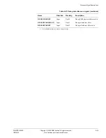
A.6
TCM interface signals
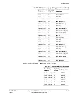
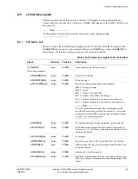
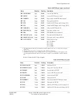
Table A-8 shows the ATCM port signals.
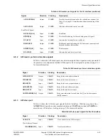
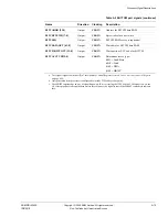
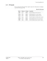
Table A-9 shows the B0TCM port signals.
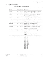
Table A-8 ATCM port signals
Name
Direction
Clocking
Description
ATCDATAIN [63:0]
Input
CLKIN
Data from ATCM
ATCPARITYIN [13:0]
Input
CLKIN
Parity or ECC code from ATCM
ATCERROR
Input
CLKIN
Error detected by ATCM
a
ATCWAIT
Input
CLKIN
Wait from ATCM
ATCLATEERROR
Input
CLKIN
Late error from ATCM
a
ATCRETRY
Input
CLKIN
Access to ATCM must be retried
a
ATCADDRPTY
Output
CLKIN
Parity formed from ATCM address output
b
ATCEN0
Output
CLKIN
Enable for ATCM lower word, bit range [31:0]
ATCEN1
Output
CLKIN
Enable for ATCM upper word, bit range [64:32]
ATCWE
Output
CLKIN
Write enable for ATCM
ATCADDR [22:3]
Output
CLKIN
Address for ATCM data RAM
ATCBYTEWR [7:0]
Output
CLKIN
Byte strobes for direct write
ATCSEQ
Output
CLKIN
ATCM RAM access is sequential
ATCDATAOUT [63:0]
Output
CLKIN
Write data for ATCM data RAM
ATCPARITYOUT [13:0]
Output
CLKIN
Write parity or ECC code for ATCM
ATCACCTYPE[2:0]
Output
CLKIN
Determines access type:
b001 = Load/Store
b010 = Fetch
b100 = DMA
b100 = MBIST
c
.
a. This signal is ignored when bit [0] of the Auxiliary Control Register is set to 0, see
c1, Auxiliary Control
Register
on page 4-38.
b. Only generated if the processor is configured to include TCM address bus parity.
c. The MBIST interface has no way of signalling a wait. If it is accessing the TCM, and the TCM signals a wait,
the AXI slave pipeline stalls and the data arrives later. However, no signal is sent to the MBIST controller to
indicate this.
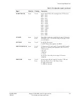
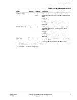
Table A-9 B0TCM port signals
Name
Direction
Clocking
Description
B0TCDATAIN [63:0]
Input
CLKIN
Data from B0TCM
B0TCPARITYIN [13:0]
Input
CLKIN
Parity or ECC code from B0TCM
B0TCERROR
Input
CLKIN
Error detected by B0TCM
a
B0TCWAIT
Input
CLKIN
Wait from B0TCM