background image

Debug 

ARM DDI 0363E

Copyright © 2009 ARM Limited. All rights reserved.

11-57

ID013010

Non-Confidential, Unrestricted Access

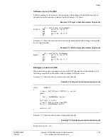
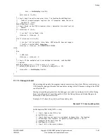
{

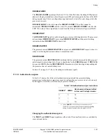
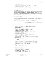
// Step 1. Poll DSCR until DTRRXfull is clear.
repeat
{

dscr := ReadDebugRegister(34);

}
until (!(dscr & (1<<30)));
// Step 2. Write the value to DTRRX.
WriteDebugRegister(32, dtr_val);

}

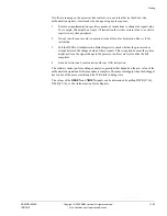
While the processor is running, if the DCC is used as a data channel, it might be appropriate to 
poll the DCC regularly.

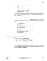
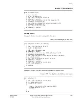
Example 11-6 shows the code for polling the DCC.

Example 11-6 Polling the DCC (host end)

PollDCC
{

dscr := ReadDebugRegister(34);
if (dscr & (1<<29))
{

// DTRTX (target -> host transfer register) full
dtr := ReadDebugRegister(35)
ProcessTargetToHostWord(dtr);

}
if (!(dscr & (1<<30)))
{

// DTRRX (host -> target transfer register) empty
dtr := GetNextHostToTargetWord()
WriteDebugRegister(32, dtr);

}

}

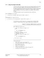
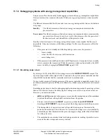
11.11.2 Programming breakpoints and watchpoints

This section describes the following operations:

Programming simple breakpoints and the byte address select

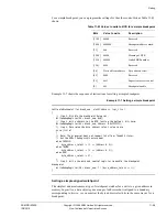
Setting a simple aligned watchpoint

 on page 11-58

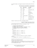
Setting a simple unaligned watchpoint

 on page 11-59.

Programming simple breakpoints and the byte address select

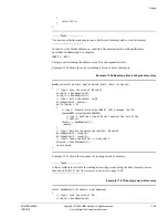
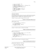
When programming a simple breakpoint, you must set the byte address select bits in the control 
register appropriately. For a breakpoint in ARM state, this is simple. For Thumb state, you must 
calculate the value based on the address.

Summary of Contents for Cortex r1p3

Page 1: ...Copyright 2009 ARM Limited All rights reserved ARM DDI 0363E ID013010 Cortex R4 and Cortex R4F Revision r1p3 Technical Reference Manual ...

Page 2: ...ntended only to assist the reader in the use of the product ARM shall not be liable for any loss or damage arising from the use of any information in this document or any error or omission in such information or any incorrect use of the product Some material in this document is based on ANSI IEEE Std 754 1985 IEEE Standard for Binary Floating Point Arithmetic The IEEE disclaims any responsibility ...

Page 3: ...s of the processor 1 11 1 5 Power management 1 12 1 6 Configurable options 1 13 1 7 Execution pipeline stages 1 17 1 8 Redundant core comparison 1 19 1 9 Test features 1 20 1 10 Product documentation design flow and architecture 1 21 1 11 Product revision information 1 24 Chapter 2 Programmer s Model 2 1 About the programmer s model 2 2 2 2 Instruction set states 2 3 2 3 Operating modes 2 4 2 4 Da...

Page 4: ...ection Unit 7 1 About the MPU 7 2 7 2 Memory types 7 7 7 3 Region attributes 7 9 7 4 MPU interaction with memory system 7 11 7 5 MPU faults 7 12 7 6 MPU software accessible registers 7 13 Chapter 8 Level One Memory System 8 1 About the L1 memory system 8 2 8 2 About the error detection and correction schemes 8 4 8 3 Fault handling 8 7 8 4 About the TCMs 8 13 8 5 About the caches 8 18 8 6 Internal ...

Page 5: ...rocessing instructions 14 7 14 4 QADD QDADD QSUB and QDSUB instructions 14 9 14 5 Media data processing 14 10 14 6 Sum of Absolute Differences SAD 14 11 14 7 Multiplies 14 12 14 8 Divide 14 14 14 9 Branches 14 15 14 10 Processor state updating instructions 14 16 14 11 Single load and store instructions 14 17 14 12 Load and Store Double instructions 14 20 14 13 Load and Store Multiple instructions ...

Page 6: ...tricted Access A 7 Dual core interface signals A 16 A 8 Debug interface signals A 17 A 9 ETM interface signals A 19 A 10 Test signals A 20 A 11 MBIST signals A 21 A 12 Validation signals A 22 A 13 FPU signals A 23 Appendix B ECC Schemes B 1 ECC scheme selection guidelines B 2 Appendix C Revisions Glossary ...

Page 7: ... Table 4 1 System control coprocessor register functions 4 3 Table 4 2 Summary of CP15 registers and operations 4 9 Table 4 3 Main ID Register bit functions 4 15 Table 4 4 Cache Type Register bit functions 4 16 Table 4 5 TCM Type Register bit functions 4 16 Table 4 6 MPU Type Register bit functions 4 17 Table 4 7 Processor Feature Register 0 bit functions 4 19 Table 4 8 Processor Feature Register ...

Page 8: ... Register bit functions 4 59 Table 4 41 Slave Port Control Register bit functions 4 60 Table 4 42 nVAL IRQ Enable Set Register bit functions 4 62 Table 4 43 nVAL FIQ Enable Set Register bit functions 4 63 Table 4 44 nVAL Reset Enable Set Register bit functions 4 64 Table 4 45 nVAL Debug Request Enable Set Register bit functions 4 65 Table 4 46 nVAL IRQ Enable Clear Register bit functions 4 66 Tabl...

Page 9: ...acheable Normal memory 9 15 Table 9 18 STR or STM1 to Cacheable write through or Non cacheable Normal memory 9 16 Table 9 19 AXI transaction splitting all six words in same cache line 9 16 Table 9 20 AXI transaction splitting data in two cache lines 9 17 Table 9 21 Non cacheable LDR or LDM1 crossing a cache line boundary 9 17 Table 9 22 Cacheable write through or Non cacheable STRH crossing a cach...

Page 10: ... 11 36 Table 11 34 Peripheral ID Register 1 functions 11 37 Table 11 35 Peripheral ID Register 2 functions 11 37 Table 11 36 Peripheral ID Register 3 functions 11 37 Table 11 37 Peripheral ID Register 4 functions 11 37 Table 11 38 Component Identification Registers 11 38 Table 11 39 Processor behavior on debug events 11 40 Table 11 40 Values in link register after exceptions 11 42 Table 11 41 Read...

Page 11: ...t single precision data processing instructions cycle timing behavior 14 32 Table 14 27 Floating point double precision data processing instructions cycle timing behavior 14 33 Table 14 28 Permitted instruction combinations 14 35 Table 15 1 Miscellaneous input ports timing parameters 15 3 Table 15 2 Configuration input port timing parameters 15 3 Table 15 3 Interrupt input ports timing parameters ...

Page 12: ...opyright 2009 ARM Limited All rights reserved xii ID013010 Non Confidential Unrestricted Access Table A 18 FPU signals A 23 Table C 1 Differences between issue B and issue C C 1 Table C 2 Differences between issue C and issue D C 3 ...

Page 13: ...ry sequence 2 21 Figure 3 1 Power on reset 3 7 Figure 3 2 AXI interface clocking 3 9 Figure 4 1 System control and configuration registers 4 4 Figure 4 2 MPU control and configuration registers 4 5 Figure 4 3 Cache control and configuration registers 4 6 Figure 4 4 TCM control and configuration registers 4 6 Figure 4 5 System performance monitor registers 4 7 Figure 4 6 System validation registers...

Page 14: ... format 4 56 Figure 4 41 BTCM Region Registers 4 58 Figure 4 42 ATCM Region Registers 4 59 Figure 4 43 Slave Port Control Register 4 60 Figure 4 44 nVAL IRQ Enable Set Register format 4 62 Figure 4 45 nVAL FIQ Enable Set Register format 4 63 Figure 4 46 nVAL Reset Enable Set Register format 4 64 Figure 4 47 nVAL Debug Request Enable Set Register format 4 65 Figure 4 48 nVAL IRQ Enable Clear Regist...

Page 15: ...ock Status Register format 11 29 Figure 11 13 Authentication Status Register format 11 29 Figure 11 14 PRCR format 11 30 Figure 11 15 PRSR format 11 31 Figure 11 16 Claim Tag Set Register format 11 33 Figure 11 17 Claim Tag Clear Register format 11 34 Figure 11 18 Lock Status Register format 11 34 Figure 11 19 Device Type Register format 11 35 Figure 12 1 FPU register bank 12 3 Figure 12 2 Floatin...

Page 16: ...All rights reserved xvi ID013010 Non Confidential Unrestricted Access Preface This preface introduces the Cortex R4 and Cortex R4F Technical Reference Manual It contains the following sections About this book on page xvii Feedback on page xxi ...

Page 17: ...tus of the product Intended audience This book is written for system designers system integrators and programmers who are designing or programming a System on Chip SoC that uses the processor Using this book This book is organized into the following chapters Chapter 1 Introduction Read this for an introduction to the processor and descriptions of the major functional blocks Chapter 2 Programmer s ...

Page 18: ...meters applicable to the processor Chapter 14 Cycle Timings and Interlock Behavior Read this for a description of the instruction cycle timing and instruction interlocks Appendix A Processor Signal Descriptions Read this for a description of the inputs and outputs of the processor Appendix B ECC Schemes Read this for a description of how to select the Error Checking and Correction ECC scheme depen...

Page 19: ...ns when they occur have clear labels You must not assume any timing information that is not explicit in the diagrams Shaded bus and signal areas are undefined so the bus or signal can assume any value within the shaded area at that time The actual level is unimportant and does not affect normal operation Key to timing diagram conventions Signals The signal conventions are Signal level The level of...

Page 20: ...Mv7 A and ARMv7 R edition ARM DDI 0406 ARM PrimeCell Vectored Interrupt Controller PL192 Technical Reference Manual ARM DDI 0273 Cortex R4 and Cortex R4F Integration Manual ARM DII 0130 Cortex R4 and Cortex R4F Configuration and Sign off Guide ARM DII 0185 CoreSight DAP Lite Technical Reference Manual ARM DDI 0316 CoreSight ETM R4 Technical Reference Manual ARM DII 0367 RealView Compilation Tools ...

Page 21: ...s product contact your supplier and give The product name The product revision or version An explanation with as much information as you can provide Include symptoms if appropriate Feedback on this book If you have any comments on this book send an e mail to errata arm com Give the title the number the relevant page number s to which your comments apply a concise explanation of your comments ARM a...

Page 22: ...ut the processor on page 1 2 About the architecture on page 1 3 Components of the processor on page 1 4 External interfaces of the processor on page 1 11 Power management on page 1 12 Configurable options on page 1 13 Execution pipeline stages on page 1 17 Redundant core comparison on page 1 19 Test features on page 1 20 Product documentation design flow and architecture on page 1 21 Product revis...

Page 23: ...PU The Cortex R4F processor is a Cortex R4 processor that includes the FPU A Harvard Level one L1 memory system with optional Tightly Coupled Memory TCM interfaces with support for error correction or parity checking memories optional caches with support for optional error correction schemes optional ARMv7 R architecture Memory Protection Unit MPU optional parity and Error Checking and Correction ...

Page 24: ...hitecture This includes the VFPv3 instruction set The ARMv7 R architecture provides 32 bit ARM and 16 bit and 32 bit Thumb instruction sets including a range of Single Instruction Multiple Data SIMD Digital Signal Processing DSP instructions that operate on 16 bit or 8 bit data values in 32 bit registers See the ARM Architecture Reference Manual ARMv7 A and ARMv7 R edition for more information on ...

Page 25: ...s from the memory system predicts branches and passes instructions to the Data Processing Unit DPU The DPU executes all instructions and uses the Load Store Unit LSU for data memory transfers The PFU and LSU interface to the L1 memory system that contains L1 instruction and data caches and an interface to a L2 system The L1 memory can also contain optional TCM interfaces Processor Level two interf...

Page 26: ...s and L2 memory interfaces 1 3 3 Prefetch unit The PFU obtains instructions from the instruction cache the TCMs or from external memory and predicts the outcome of branches in the instruction stream See Chapter 5 Prefetch Unit for more information Branch prediction The branch predictor is a global type that uses history registers and a 256 entry pattern history table Return stack The PFU includes ...

Page 27: ...attributes for embedded control applications You can configure the MPU to have eight or twelve regions each with a minimum resolution of 32 bytes MPU regions can overlap and the highest numbered region has the highest priority The MPU checks for protection and memory attributes and some of these can be passed to an external L2 memory system For more information see Chapter 7 Memory Protection Unit...

Page 28: ... memory using an AXI master and AXI slave port AXI master interface The AXI master interface provides a high bandwidth interface to second level caches on chip RAM peripherals and interfaces to external memory It consists of a single AXI port with a 64 bit read channel and a 64 bit write channel for instruction and data fetches The AXI master can run at the same frequency as the processor or at a ...

Page 29: ...lects various processor signals and drives these signals from the processor The interface is unidirectional and runs at the full speed of the processor The ETM interface connects directly to the external ETM unit without any additional glue logic You can disable the ETM interface for power saving For more information see the CoreSight ETM R4 Technical Reference Manual Real time debug facilities Th...

Page 30: ...through the system control coprocessor For more information see System control and configuration on page 4 4 1 3 8 Interrupt handling Interrupt handling in the processor is compatible with previous ARM architectures but has several additional features to improve interrupt performance for real time applications VIC port The core has a dedicated port that enables an external interrupt controller suc...

Page 31: ...right 2009 ARM Limited All rights reserved 1 10 ID013010 Non Confidential Unrestricted Access RFE Return from exception using data from the stack CPS Change processor state such as interrupt mask setting and clearing and mode changes ...

Page 32: ... ETM interface You can connect an ETM R4 to the processor through the ETM interface The ETM R4 provides instruction and data trace for the processor For more information on how the ETM R4 connects to the processor see the CoreSight ETM R4 Technical Reference Manual All outputs are driven directly from a register unless specified otherwise All signals are relative to CLKIN unless specified otherwis...

Page 33: ...y of the processor is available Standby mode This mode disables most of the clocks of the device while keeping the device powered up This reduces the power drawn to the static leakage current and the minimal clock power overhead required to enable the device to wake up from the Standby mode Shutdown mode This mode has the entire device powered down All state including cache and TCM state must be s...

Page 34: ...nfiguration or pin configuration Redundant core Single core no redundancy Build Dual core redundant In phase clocks Out of phase clocks Build Instruction cache No i cache Build i cache included No error checking Parity error checking 64 bit ECC error checking Build 4KB 4x1KB ways 8KB 4x2KB ways 16KB 4x4KB ways 32KB 4x8KB ways 64KB 4x16KB ways Build Data cache No d cache Build d cache included No e...

Page 35: ...or 2x4MB Pin Interleaved on 64 bit granularity in memory Adjacent in memory Pin Instruction endianness Little endian Build Pin configured Little endian Big endian Pin Floating point VFP No FPU Build FPU includeda MPU No MPU Build MPU included 8 MPU regions 12 MPU regions Build TCM bus parity No TCM address and control bus parity Build TCM address and control bus parity generated AXI bus parity No ...

Page 36: ...in Enabled Parity typed Odd parity Pin Even parity a Only available with the Cortex R4F processor b Only if the relevant TCM port s are included c Only if at least one TCM port is included and uses ECC error checking d Only relevant if at least one TCM port is included and uses parity error checking one of the caches includes parity checking or AXI or TCM bus parity is included Table 1 1 Configura...

Page 37: ...endently B0TCMECEN B1TCMECEN TCM load store 64 read modify write behavior ATCM load store 64 enableb ATCMRMW BTCM load store 64 enableb BTCMRMW a Can only be enabled if the appropriate TCM is configured with the appropriate error checking scheme and the appropriate number of ports b Can only be enabled if the appropriate TCM is not configured with 32 bit ECC Table 1 2 Configurable options at reset...

Page 38: ...tch where data is returned from instruction memory Pd Pre decode where instructions are formatted and branch prediction occurs De Instruction decode Figure 1 3 shows the Issue and Execution pipeline stages for the Cortex R4 processor Figure 1 3 Cortex R4 Issue and Execution pipeline stages Figure 1 4 on page 1 18 shows the Issue and Execution pipeline stages for the Cortex R4F processor Fe1 Fe2 Pd...

Page 39: ...2 Second stage of data memory access The names of the floating point pipeline stages and their functions are F0 Floating point register read F1 First stage of floating point execution F2 Second stage of floating point execution Fwr Floating point writeback The pipeline structure provides a pipelined 2 cycle memory access and single cycle load use penalty This enables integration with slow RAM bloc...

Page 40: ...h those of the master core If a fault occurs in the logic of either core because of radiation or circuit failure this is detected by the comparison logic Used in conjunction with the RAM error detection schemes this can help protect the system from faults The inputs DCCMINP 7 0 and DCCMINP2 7 0 and the outputs DCCMOUT 7 0 and DCCMOUT2 7 0 enable the comparison logic inside the processor to communi...

Page 41: ... present in the processor design which improves the potential frequency compared to adding multiplexors to the RAM modules See the Cortex R4 and Cortex R4F Integration Manual for more information about this interface and how to control it In addition you can use the AXI slave interface to read and write the cache and TCM RAMs You can use this feature to test the cache RAMs in a running system This...

Page 42: ...igure the Register Transfer Level RTL with the build configuration options the processes to sign off the configured RTL and final macrocell The ARM product deliverables include reference scripts and information about using them to implement your design Reference methodology documentation from your EDA tools vendor complements the CSG The CSG is a confidential book that is only available to license...

Page 43: ...rocell includes both BTCM ports the integrator can choose how many ports to actually use and therefore how many RAMs must be integrated with the macrocell If the integrator only wishes to use one BTCM port they can connect RAM to the B0TCM port only and tie the ENTCM1IF input to zero to indicate that the B1TCM is not available Software configuration The programmer configures the processor by progr...

Page 44: ... a System on Chip SoC It facilitates development of embedded processors with multiple peripherals IEEE 754 This is the IEEE Standard for Binary Floating Point Arithmetic An architecture specification typically defines a number of versions and includes features that are either optional or partially specified The TRM describes which architectures are used including which version is implemented and t...

Page 45: ... Main ID Register MIDR This register is accessible by software and identifies the part the variant and the revision See c0 Main ID Register on page 4 14 A copy of this register can also be read by a debugger through the debug APB interface See Processor ID Registers on page 11 32 Debug ID Register DIDR This register can be read by a debugger through the debug APB interface and by software It ident...

Page 46: ...ues that the processor implements for the fields in these registers For details of the possible values and their meanings for these fields see the ARM Architecture Reference Manual Table 1 3 ID values for different product versions ID value r0p0 r0p1 r0p2 r0p3 r1p0 r1p1 r1p2 r1p3 Variant field Main ID Register 0x0 0x0 0x0 0x0 0x1 0x1 0x1 0x1 Revision field Main ID Register 0x0 0x1 0x2 0x3 0x0 0x1 ...

Page 47: ...processor It contains the following sections About the programmer s model on page 2 2 Instruction set states on page 2 3 Operating modes on page 2 4 Data types on page 2 5 Memory formats on page 2 6 Registers on page 2 7 Program status registers on page 2 10 Exceptions on page 2 16 Acceleration of execution environments on page 2 27 Unaligned and mixed endian data access support on page 2 28 Big e...

Page 48: ... range of 32 bit instructions For more information on the ARM and Thumb instruction sets see the ARM Architecture Reference Manual This chapter describes some of the main features of the architecture but for a complete description see the ARM Architecture Reference Manual This chapter also makes reference to older versions of the ARM architecture that the processor does not implement These referen...

Page 49: ...truction set state of the processor can be switched between ARM state and Thumb state Using the BX and BLX instructions by a load to the PC or with a data processing instruction that does not set flags with the PC as the destination register Switching state is described in the ARM Architecture Reference Manual Note When the BXJ instruction is used the processor invokes the BX instruction Automatic...

Page 50: ...g a fast interrupt Interrupt IRQ mode is entered on taking a normal interrupt Supervisor SVC mode is a protected mode for the operating system and is entered on taking a Supervisor Call SVC formerly SWI Abort ABT mode is entered after a data or instruction abort System SYS mode is a privileged user mode for the operating system Undefined UND mode is entered when an Undefined instruction exception ...

Page 51: ...ta value represents an integer in the range 2N 1 to 2N 1 1 using two s complement format For best performance you must align these data types in memory as follows doubleword quantities aligned to 8 byte boundaries doubleword aligned word quantities aligned to 4 byte boundaries word aligned halfword quantities aligned to 2 byte boundaries halfword aligned byte quantities can be placed on any byte b...

Page 52: ...rence Manual 2 5 1 Byte invariant big endian format In byte invariant big endian BE 8 format the processor stores the most significant byte of a word at the lowest numbered byte and the least significant byte at the highest numbered byte Figure 2 1 shows byte invariant big endian BE 8 format Figure 2 1 Byte invariant big endian BE 8 format 2 5 2 Little endian format In little endian format the low...

Page 53: ...ses register R13 as a Stack Pointer SP The SRS and RFE instructions use Register R13 Link Register Register R14 is used as the subroutine Link Register LR Register R14 receives the return address when a Branch with Link BL or BLX instruction is executed You can use R14 as a general purpose register at all other times The corresponding banked registers R14_svc R14_irq R14_fiq R14_abt and R14_und si...

Page 54: ...tifiers FIQ mode has seven banked registers mapped to R8 R14 R8_fiq R14_fiq As a result many FIQ handlers do not have to save any registers The Supervisor Abort IRQ and Undefined modes each have alternative mode specific registers mapped to R13 and R14 permitting a private stack pointer and link register for each mode Figure 2 3 on page 2 9 shows the register set and those registers that are banke...

Page 55: ...struction enables you to add high register values to low register values For more information see the ARM Architecture Reference Manual General registers and program counter System and User Program status registers banked register Supervisor Abort IRQ Undefined R0 R1 R2 R3 R4 R5 R6 R7 R8 R9 R10 R11 R12 R13 R14 R15 FIQ R0 R1 R2 R3 R4 R5 R6 R7 R8_fiq R9_fiq R10_fiq R11_fiq R12_fiq R13_fiq R14_fiq R1...

Page 56: ... E bit on page 2 13 The A bit on page 2 13 The I and F bits on page 2 13 The T bit on page 2 13 The M bits on page 2 14 2 7 1 The N Z C and V bits The N Z C and V bits are the condition code flags You can optionally set them with arithmetic and logical operations and also with MSR instructions and MRC instructions to R15 The processor tests these flags in accordance with an instruction s condition...

Page 57: ... on the status of the Q flag To determine the status of the Q flag you must read the PSR into a register and extract the Q flag from this For information of how the Q flag is set and cleared see individual instruction definitions in the ARM Architecture Reference Manual 2 7 3 The IT bits IT 7 5 encodes the base condition code for the current IT block if any It contains b000 when no IT block is act...

Page 58: ... bits for individual halfwords or bytes of the result as Table 2 2 shows Table 2 2 GE 3 0 settings GE 3 GE 2 GE 1 GE 0 Instruction A op B greater than or equal to C A op B greater than or equal to C A op B greater than or equal to C A op B greater than or equal to C Signed SADD16 31 16 31 16 0 31 16 31 16 0 15 0 15 0 0 15 0 15 0 0 SSUB16 31 16 31 16 0 31 16 31 16 0 15 0 15 0 0 15 0 15 0 0 SADDSUBX...

Page 59: ...prior to ARMv6 specify this bit as SBZ This ensures no endianness reversal on loads or stores 2 7 8 The A bit The A bit is set automatically It disables imprecise Data Aborts For more information on how to use the A bit see Imprecise abort masking on page 2 23 2 7 9 The I and F bits The I and F bits are the interrupt disable bits when the I bit is set IRQ interrupts are disabled when the F bit is ...

Page 60: ...ten as a side effect of another instruction If an MSR instruction tries to modify these bits the results are architecturally Unpredictable In the processor these bits are not affected The bits in Figure 2 4 on page 2 10 that are in this category are the execution state bits 26 24 15 10 and 5 Bits that can only be modified from Privileged modes and that instructions completely protect from modifica...

Page 61: ...grammer sModel ARM DDI 0363E Copyright 2009 ARM Limited All rights reserved 2 15 ID013010 Non Confidential Unrestricted Access Bits in Figure 2 4 on page 2 10 that are in this category are A I F and M 4 0 ...

Page 62: ... is handled differently to normal See Exceptions in debug state on page 11 47 for more details 2 8 1 Exception entry and exit summary Table 2 4 summarizes the PC value preserved in the relevant R14 on exception entry and the recommended instruction for exiting the exception handler Table 2 4 Exception entry and exit Exception or entry Recommended return instruction Previous state Notes ARMR14_x Th...

Page 63: ...he PC to fetch the next instruction from the relevant exception vector The processor can also set the interrupt disable flags to prevent otherwise unmanageable nesting of exceptions Leaving an exception When an exception has completed the exception handler must move the LR minus an offset to the PC The offset varies according to the type of exception as Table 2 4 on page 2 16 shows Typically the r...

Page 64: ...pin when asserted and not masked causes the processor to take the appropriate type of interrupt exception See Exceptions on page 2 16 for more information The CPSR F and CPSR I bits control masking of fast and normal interrupts respectively A number of features exist to improve the interrupt latency that is the time taken between the assertion of the interrupt input and the execution of the interr...

Page 65: ...nterrupts FIQ and IRQ interrupts are automatically masked by setting the CPSR F and CPSR I bits when an FIQ occurs You can use nested interrupts but it is up to you to save any corruptible registers and to re enable interrupts Non maskable fast interrupts When NMFI behavior is enabled FIQ interrupts cannot be masked by software Enabling NMFI behavior ensures that when the FIQ mask that is the CPSR...

Page 66: ...errupt request outputs to the processor the ability to mask out particular interrupt requests prioritization of interrupt sources for interrupt nesting In a system with an interrupt controller with these features software is still required to determine from the interrupt controller which interrupt source is requesting service determine where the service routine for that interrupt source is loaded ...

Page 67: ...stem Control Register on page 4 35 LR_fiq RA 4 CPSR 4 0 FIQ mode CPSR 5 TE CPSR 7 1 CPSR 6 1 SPSR_fiq CPSR V 1 FALSE TRUE FALSE nFIQ F nIRQ I nFIQ F VE 1 FALSE V 1 TRUE PC 31 0 Handler address provided by VIC Acknowledge address to VIC TRUE FALSE Is VIC ready to provide handler address FALSE TRUE TRUE Start handshake with VIC LR_irq RA 4 SPSR_irq CPSR CPSR 4 0 IRQ mode FALSE CPSR 7 1 CPSR 5 TE VE ...

Page 68: ...because a branch occurs while it is in the pipeline the abort does not take place All prefetch aborts are precise Data aborts An error occurring on a data memory access can generate a data abort If the instruction generating the memory access is not executed for example because it fails its condition codes or is interrupted the data abort does not take place A Data Abort DABT can be either precise...

Page 69: ...atically set when abort IRQ or FIQ exceptions are taken and on reset You must only clear the A bit in an abort handler after the state information has either been stacked to memory or is no longer required Only one pending imprecise abort of each imprecise abort type is supported The processor supports the following pending imprecise aborts Imprecise external abort If a subsequent imprecise extern...

Page 70: ...iants and unaligned LDR STR LDRH and STRH Abort handler If you configure the processor with parity or ECC on the caches or the TCMs and the abort handler is in one of these memories then it is possible for a parity or ECC error to occur in the abort handler If the error is not recoverable then a precise abort occurs and the processor loops until the next interrupt The LR and SPSR values for the or...

Page 71: ...2 bit instructions in Thumb state After testing the SPSR and determining the instruction was executed in Thumb state the Undefined handler must use the following pseudo code or equivalent to obtain this information addr R14_undef 2 instr Memory addr 2 if instr 11 28 32 bit instruction instr instr 16 Memory addr 2 2 if emulating so return after instruction wanted R14_undef 2 After this instr holds ...

Page 72: ...s Table 2 5 shows Table 2 6 shows the exception vector addresses and entry conditions for the different exception types Table 2 5 Configuration of exception vector address locations Value of V bit Exception vector base location 0 0x00000000 1 HIVECS 0xFFFF0000 Table 2 6 Exception vectors Exception Offset from vector base Mode on entry A bit on entry F bit on entry I bit on entry Reset 0x00 Supervi...

Page 73: ...egister instruction summary and the response to the instructions Note Because no hardware acceleration is present in the processor when the BXJ instruction is used the BX instruction is invoked Table 2 7 Jazelle register instruction summary Register Instruction Response Jazelle ID MRC p14 7 Rd c0 c0 0 MCR p14 7 Rd c0 c0 0 Read as zero Ignore writes Jazelle main configuration MRC p14 7 Rd c2 c0 0 M...

Page 74: ...d memory accesses Unaligned memory accesses was introduced with ARMv6 Bit 22 of c1 Control Register is always 1 The processor supports byte invariant big endianness BE 8 and little endianness LE The processor does not support word invariant big endianness BE 32 Bit 7 of c1 Control Register is always 0 For more information on unaligned and mixed endian data access support see the ARM Architecture R...

Page 75: ...he setting of the CFGIE pin This is reflected in bit 31 of the System Control Register For more information see c1 System Control Register on page 4 35 Note The facility to use big endian or little endian instruction format is an implementation option and you can therefore remove it in specific implementations If this facility is not present the CFGIE pin is still reflected in the System Control R...

Page 76: ...software on the processor it must be reset and initialized including loading the appropriate software configuration This chapter describes the signals for clocking and resetting the processor and the steps that the software must take to initialize the processor after reset It contains the following sections Initialization on page 3 2 Resets on page 3 6 Reset modes on page 3 7 Clocking on page 3 9 ...

Page 77: ...CM on page 3 3 3 1 1 MPU If the processor has been built with an MPU before you can use it you must program and enable at least one of the regions enable the MPU in the System Control Register See c6 MPU memory region programming registers on page 4 49 Do not enable the MPU unless at least one MPU region is programmed and active If the MPU is enabled before using the TCM interfaces you must progra...

Page 78: ... application to use This section describes various ways that you can perform data preloading You can also configure the processor to use the TCMs from reset Preloading TCMs You can write data to the TCMs using either store instructions or the AXI slave interface Depending on the method you choose you might require particular hardware on the SoC that you are using boot code a debugger connected to ...

Page 79: ...s If the error scheme is parity any write transaction can be used If the error scheme is 32 bit ECC the write transactions must start at a 32 bit aligned addresses and write a continuous block of memory containing a multiple of 4 bytes All bytes in the block must be written that is have their byte lane strobe asserted If the error scheme is 64 bit ECC the write transactions must start at a 64 bit ...

Page 80: ... TCM interfaces from reset and to select the address at which each TCM appears from reset See TCM initialization on page 8 16 for more details This enables you to configure the processor to boot from TCM but to do this the TCM must first be preloaded with the boot code The nCPUHALT pin can be asserted while the processor is in reset to stop the processor from fetching and executing instructions af...

Page 81: ...l resets processor debug logic and CoreSight ETM R4 nSYSPORESET This signal is the reset that initializes the entire processor including CP14 debug logic and the APB debug logic See CP14 registers reset on page 11 23 for information nCPUHALT This signal stops the processor from fetching instructions after reset All of these are active LOW signals that reset logic in the processor You must take car...

Page 82: ...wer on reset the leading or falling edge of the reset signals nRESET and nSYSPORESET does not have to be synchronous to CLKIN Because the nRESET and nSYSPORESET signals are synchronized within the processor you do not have to synchronize these signals Figure 3 1 shows the application of power on reset Figure 3 1 Power on reset ARM recommends that you assert the reset signals for at least four CLKI...

Page 83: ...sor you do not have to synchronize this signal 3 3 3 Normal operation During normal operation neither processor reset nor power on reset is asserted If the Embedded ICE RT is not used the value of PRESETDBGn does not matter 3 3 4 Halt operation When nCPUHALT is asserted and nSYSPORESET and nRESET deasserted the processor is out of reset but the PFU is inhibited from fetching instructions For examp...

Page 84: ...o AXI systems that are synchronous to the processor clock CLKIN even if this might be at a lower frequency This means that every rising edge on the AXI system clock must be synchronous to a rising edge on CLKIN The AXI master interface clock enable signal ACLKENM and the AXI slave interface clock enable signal ACLKENS must be asserted on every CLKIN rising edge for which there is a simultaneous ri...

Page 85: ...stricted Access Chapter 4 System Control Coprocessor This chapter describes the purpose of the system control coprocessor its structure operation and how to use it It contains the following sections About the system control coprocessor on page 4 2 System control coprocessor registers on page 4 9 ...

Page 86: ...performance monitoring The system control coprocessor does not exist in a distinct physical block of logic 4 1 1 System control coprocessor functional groups The system control coprocessor appears as a set of registers that you can write to and read from Some of the registers permit more than one type of operation The functional groups for the registers are System control and configuration on page...

Page 87: ...tibility Thread And Process ID c13 Thread and Process ID Registers on page 4 61 MPU control and configuration Data Fault Status c5 Data Fault Status Register on page 4 45 Auxiliary Fault Status c5 Auxiliary Fault Status Registers on page 4 47 Instruction Fault Status c5 Instruction Fault Status Register on page 4 46 Instruction Fault Address c6 Instruction Fault Address Register on page 4 49 Data ...

Page 88: ...ystem functionality as a set of addresses for processes in memory TCM control and configuration TCM Status c0 TCM Type Register on page 4 16 Region c9 BTCM Region Register on page 4 57 c9 TCM Selection Register on page 4 59 System performance monitoring Performance monitoring Chapter 6 Events and Performance Monitor Validation System validation Validation Registers on page 4 62 a Known as the ID C...

Page 89: ...nd configuration registers provide information on the size and architecture of the instruction and data caches control cache maintenance operations that include clean and invalidate caches drain and flush buffers and address translation override cache behavior during debug or interruptible cache operations The cache control and configuration registers consist of three read only registers one read ...

Page 90: ...f the TCMs as a set of bits that enable specific TCM functionality as a set of addresses that define the memory locations of data stored in the TCMs 4 1 6 System performance monitor The performance monitor registers control the monitoring operation count events The system performance monitor consists of 12 read write registers Figure 4 5 on page 4 7 shows the arrangement of registers in this funct...

Page 91: ...ebug requests The system validation registers consist of nine read write registers and one write only register Figure 4 6 shows the arrangement of registers Figure 4 6 System validation registers Opcode_2 CRm CRn Opcode_1 c9 0 0 c12 Overflow Flag Status Register Count Enable Set Register Count Enable Clear Register Performance Monitor Control Register Event Select Register Performance Counter Sele...

Page 92: ...rocessor ARM DDI 0363E Copyright 2009 ARM Limited All rights reserved 4 8 ID013010 Non Confidential Unrestricted Access You can only change the cache size to a size supported by the cache RAMs implemented in your design ...

Page 93: ...0 0 3 6 7 Main ID Read only 0x41xFC14xa page 4 14 1 Cache Type Read only 0x8003C003 page 4 15 2 TCM Type Read only 0x00010001 page 4 16 4 MPU Type Read only 0x00000000b page 4 17 5 Multiprocessor ID Read only 0x00000000 page 4 18 c1 0 Processor Feature 0 Read only 0x00000131 page 4 18 1 Processor Feature 1 Read only 0x00000001 page 4 19 2 Debug Feature 0 Read only 0x00010400 page 4 20 3 Auxiliary ...

Page 94: ...45 1 Instruction Fault Status Read write Unpredictable page 4 46 2 7 Undefined c1 0 Auxiliary Data Fault Status Read write Unpredictable page 4 47 c5 0 c1 1 Auxiliary Instruction Fault Status Read write Unpredictable page 4 47 2 7 Undefined c2 c15 0 7 c6 0 c0 0 Data Fault Address Read write Unpredictable page 4 48 1 Undefined 2 Instruction Fault Address Read write Unpredictable page 4 49 3 7 Undef...

Page 95: ...Undefined 6 Invalidate entire branch predictor array Write only page 4 55 7 Invalidate address from branch predictor array Write only page 4 55 c6 0 Undefined 1 Invalidate data cache line by physical address Write only page 4 55 2 Invalidate data cache line by Set Way Write only page 4 55 3 7 Undefined c7 9 0 7 c10 0 1 Clean data cache line by physical address Write only page 4 55 2 Clean data cac...

Page 96: ...n Read write d page 4 57 2 7 Undefined c2 0 TCM selection Read write 0x00000000 page 4 59 1 7 Undefined c3 c11 0 7 c12 0 Performance Monitor Control Read write 0x41141800 page 6 7 1 Count Enable Set Read write Unpredictable page 6 8 2 Count Enable Clear Read write Unpredictable page 6 9 3 Overflow Flag Status Read write Unpredictable page 6 10 4 Software Increment Write only page 6 11 c9 0 c12 5 P...

Page 97: ...rite 0x00000000 page 4 61 4 Privileged Only Thread and Process ID Read write 0x00000000 page 4 61 5 7 Undefined c13 0 c1 c15 0 7 Undefined c14 0 c0 c15 0 7 c15 0 c0 0 Secondary Auxiliary Control Read write d page 4 41 1 7 Undefined c1 0 nVAL IRQ Enable Set Read write Unpredictable page 4 62 1 nVAL FIQ Enable Set Read write Unpredictable page 4 63 2 nVAL Reset Enable Set Read write Unpredictable pa...

Page 98: ...lt Location Read write Unpredictable page 4 70 1 7 Undefined c4 0 7 c5 0 Invalidate all data cache Write only page 4 55 1 7 Undefined c6 c13 0 7 c15 0 c14 0 Cache Size Override Write only page 4 69 1 7 Undefined c15 0 7 a The value of bits 23 20 3 0 of the Main ID Register depend on product revision See the register description for more information b Reset value depends on number of MPU regions c ...

Page 99: ...r is a read only register accessible in Privileged mode only The contents of the Cache Type Register depend on the specific implementation Figure 4 8 shows the arrangement of bits in the register Figure 4 8 Cache Type Register format Table 4 3 Main ID Register bit functions Bits Field Function 31 24 Implementer Indicates implementer 0x41 ARM Limited 23 20 Variant Identifies the major revision of t...

Page 100: ...gister functions Table 4 4 Cache Type Register bit functions Bits Field Function 31 28 Always b1000 27 24 CWG Cache Write back Granule 0x0 no information provided See maximum cache line size in c0 Current Cache Size Identification Register on page 4 32 23 20 ERG Exclusives Reservation Granule 0x0 no information provided 19 16 DMinLine Indicates log2 of the number of words in the smallest cache lin...

Page 101: ...ons implemented in the processor The MPU Type Register is read only register accessible in Privileged mode only Figure 4 10 shows the arrangement of bits in the register Figure 4 10 MPU Type Register format Table 4 6 shows how the bit values correspond with the MPU Type Register functions To access the MPU Type Register read CP15 with 18 16 BTCM Specifies the number of BTCMs implemented This is al...

Page 102: ...processor ID Register read CP15 with MRC p15 0 Rd c0 c0 5 Returns Multiprocessor ID details 4 2 7 The Processor Feature Registers There are two Processor Feature Registers PFR0 and PFR1 This section describes c0 Processor Feature Register 0 PFR0 c0 Processor Feature Register 1 PFR1 on page 4 19 c0 Processor Feature Register 0 PFR0 The Processor Feature Register 0 provides information about the exe...

Page 103: ...Register 1 format Table 4 8 shows how the bit values correspond with the Processor Feature Register 1 functions Table 4 7 Processor Feature Register 0 bit functions Bits Field Function 31 16 Reserved SBZ 15 12 State3 Indicates support for Thumb Execution Environment ThumbEE 0x0 no support 11 8 State2 Indicates support for acceleration of execution environments in hardware or software 0x1 the proce...

Page 104: ...ty extension Indicates support for Security Extensions Architecture 0x0 no support 3 0 ARMv4 Programmer s model Indicates support for standard ARMv4 programmer s model 0x1 the processor supports the ARMv4 model Table 4 8 Processor Feature Register 1 bit functions continued Bits Field Function Reserved Microcontroller debug model memory mapped Trace debug model memory mapped Trace debug model copro...

Page 105: ...eature Register 0 MMFR0 c0 Memory Model Feature Register 1 MMFR1 on page 4 22 c0 Memory Model Feature Register 2 MMFR2 on page 4 24 c0 Memory Model Feature Register 3 MMFR3 on page 4 25 c0 Memory Model Feature Register 0 MMFR0 The Memory Model Feature Register 0 provides information about the memory model memory management and cache support operations of the processor The Memory Model Feature Regi...

Page 106: ...6 15 12 11 8 7 4 3 0 Reserved FCSE TCM PMSA VMSA Auxiliary Control Register Cache coherence Outer shareable Table 4 10 Memory Model Feature Register 0 bit functions Bits Field Function 31 28 Reserved SBZ 27 24 FCSE Indicates support for Fast Context Switch Extension FCSE 0x0 no support 23 20 Auxiliary Control Register Indicates support for the auxiliary registers 0x2 the processor supports the Aux...

Page 107: ...irements 0x0 no MMU present 27 24 L1 test clean operations Indicates support for test and clean operations on data cache Harvard or unified architecture 0x0 no support 23 20 L1 cache maintenance operations unified Indicates support for L1 cache entire cache maintenance operations unified architecture 0x0 no support 19 16 L1 cache maintenance operations Harvard Indicates support for L1 cache entire...

Page 108: ... operations Table 4 12 Memory Model Feature Register 2 bit functions Bits Field Function 31 28 Hardware access flag Indicates support for Hardware Access Flag 0x0 no support 27 24 WFI Indicates support for Wait For Interrupt stalling 0x1 the processor supports Wait For Interrupt 23 20 Memory barrier Indicates support for memory barrier operations 0x2 the processor supports DSB formerly DWB ISB for...

Page 109: ...l Feature Register 3 31 8 7 3 0 Reserved 4 12 11 Branch predictor maintenance operations Hierarchical cache maintenance operations by Set and Way Hierarchical cache maintenance operations by MVA Table 4 13 Memory Model Feature Register 3 bit functions Bits Field Function 31 12 Reserved SBZ 11 8 Branch predictor maintenance operations Indicates support for branch predictor maintenance operations in...

Page 110: ...e only Figure 4 19 shows the bit arrangement for Instruction Set Attributes Register 0 Figure 4 19 Instruction Set Attributes Register 0 format Table 4 14 shows how the bit values correspond with the Instruction Set Attributes Register 0 functions Reserved 31 28 27 24 23 20 19 16 15 12 11 8 7 4 3 0 Divide instructions Debug instructions Coprocessor instructions Compare and branch instructions Bitf...

Page 111: ...ement for Instruction Set Attributes Register 1 Figure 4 20 Instruction Set Attributes Register 1 format 11 8 Bitfield instructions Indicates support for bitfield instructions 0x1 the processor supports bitfield instructions BFC BFI SBFX and UBFX 7 4 Bit counting instructions Indicates support for bit counting instructions 0x1 the processor supports CLZ 3 0 Atomic instructions Indicates support fo...

Page 112: ...nstructions Indicates support for interworking instructions 0x3 the processor supports BX and T bit in PSRs BLX and PC loads have BX behavior Data processing instructions in the ARM instruction set with the PC as the destination and the S bit clear have BX like behavior 23 20 Immediate instructions Indicates support for immediate instructions 0x1 the processor supports the MOVT instruction MOV ins...

Page 113: ...cates support for PSR instructions 0x1 the processor supports MRS and MSR and the exception return forms of data processing instructions 23 20 Unsigned multiply instructions Indicates support for advanced unsigned multiply instructions 0x2 the processor supports UMULL and UMLAL UMAAL 19 16 Signed multiply instructions Indicates support for advanced signed multiply instructions 0x3 the processor su...

Page 114: ...ble branch instructions Synchronization primitive instructions SVC instructions SIMD instructions Saturate instructions Table 4 17 Instruction Set Attributes Register 3 bit functions Bits Field Function 31 28 ThumbEE extension Indicates support for ThumbEE Execution Environment extension 0x0 no support 27 24 True NOP instructions Indicates support for true NOP instructions 0x1 the processor suppor...

Page 115: ...ADD16 QADD8 QASX QSUB16 QSUB8 QSAX SADD16 SADD8 SASX SEL SHADD16 SHADD8 SHASX SHSUB16 SHSUB8 SHSAX SSAT SSAT16 SSUB16 SSUB8 SSAX SXTAB16 SXTB16 UADD16 UADD8 UASX UHADD16 UHADD8 UASX UHSUB16 UHSUB8 USAX UQADD16 UQADD8 UQASX UQSUB16 UQSUB8 UQSAX USAD8 USADA8 USAT USAT16 USUB16 USUB8 USAX UXTAB16 UXTB16 and the GE 3 0 bits in the PSRs 3 0 Saturate instructions Indicates support for saturate instructi...

Page 116: ...ter The Current Cache Size Identification Register provides the current cache size information for the instruction and data caches Architecturally there can be up to eight levels of cache containing instruction data or unified caches This processor contains L1 instruction and data caches The Cache Size Selection Register determines which Current Cache Size Identification Register to select see c0 ...

Page 117: ...3 12 2 0 W B R A W A NumSets Associativity Table 4 19 Current Cache Size Identification Register bit functions Bits Field Function 31 WT Indicates support available for write through 1 write through support availablea a See Table 4 20 for valid bit field encodings 30 WB Indicates support available for write back 1 write back support availablea 29 RA Indicates support available for read allocation ...

Page 118: ...evel ID Register format Table 4 21 shows how the bit values correspond with the Current Cache Level ID Register To access the Current Cache Level ID Register read CP15 with MRC p15 1 Rd c0 c0 1 Read Current Cache Level ID Register CL 8 CL 7 CL 6 CL 5 CL 4 CL 3 CL 2 CL 1 Reserved 31 30 29 27 26 24 23 21 20 18 17 15 14 12 11 10 8 6 5 3 2 0 LoU LoC Table 4 21 Current Cache Level ID Register bit funct...

Page 119: ...RC p15 2 Rd c0 c0 0 Read Cache Size Selection Register MCR p15 2 Rd c0 c0 0 Write Cache Size Selection Register 4 2 15 c1 System Control Register The System Control Register provides control and configuration information for memory alignment endianness protection and fault behavior MPU and cache enables and cache replacement strategy interrupts and the behavior of interrupt latency the location fo...

Page 120: ...le 0 enable ARM exception generation 1 enable Thumb exception generation The primary input TEINIT defines the reset value 29 AFE Access Flag Enable On the processor this bit is SBZ 28 TRE TEX Remap Enable On the processor this bit is SBZ 27 NMFI NMFI non maskable fast interrupt enable 0 Software can disable FIQs 1 Software cannot disable FIQs This bit is read only The configuration input CFGNMFI d...

Page 121: ...xception vectors 0 normal exception vectors selected address range 0x00000000 0x0000001C 1 high exception vectors HIVECS selected address range 0xFFFF0000 0xFFFF001C The primary input VINITHI defines the reset value 12 I Enables L1 instruction cache 0 instruction caching disabled This is the reset value 1 instruction caching enabled If no instruction cache is implemented then this bit is SBZ 11 Z ...

Page 122: ...the register Figure 4 28 Auxiliary Control Register format Table 4 24 shows how the bit values correspond with the Auxiliary Control Register functions 31 25 24 23 22 21 19 18 17 16 15 14 13 12 11 7 6 3 2 1 0 CEC 26 27 28 30 29 DIADI 10 20 DICDI DIB2DI DIB1DI B1TCMPCEN B0TCMPCEN ATCMPCEN AXISCEN 9 BP 5 8 AXISCUEN DILSM DEOLP DBHE FRCDIS RSDIS Reserved ATCMECEN B0TCMECEN B1TCMECEN DILS sMOV FDSnS F...

Page 123: ...ess enable 0 Disabled This is the reset value 1 Enabled Note When AXI slave cache access is enabled the caches are disabled and the processor cannot run any cache maintenance operations If the processor attempts a cache maintenance operation an Undefined instruction exception is taken 23 AXISCUEN AXI slave cache RAM non privileged access enable 0 Disabled This is the reset value 1 Enabled 22 DILSM...

Page 124: ...s therefore redundant for ASICs 11 DNCH Disable data forwarding for Non cacheable accesses in the AXI master 0 Normal operation This is the reset value 1 Disable data forwarding for Non cacheable accesses 10 FORA Force outer read allocate ORA for outer write allocate OWA regions 0 No forcing of ORA This is the reset value 1 ORA forced for OWA regions 9 FWT Force write through WT for write back WB ...

Page 125: ...nly Note This register is implemented from the r1pm releases of the processor Attempting to access this register in r0pm releases of the processor results in an Undefined Instruction exception Figure 4 29 on page 4 42 shows the arrangement of bits in the register 2 B1TCMECEN B1TCM external error enable 0 Disabled 1 Enabled The primary input ERRENRAM 2 defines the reset value 1 B0TCMECEN B0TCM exte...

Page 126: ...is value on revisions r1p2 or earlier of the processor 1 Disabled Most hard errors in the caches are fatal This is the reset value See Hard errors on page 8 5 for more information 21 DR2Bb Enable random 2 bit error generation in cache RAMs This bit has no effect unless ECC is configured see Configurable options on page 1 13 0 Disabled This is the reset value 1 Enabled Note This bit controls error ...

Page 127: ...t value 1 Propagate floating point underflow exception flag FPSCR UFC to output FPUFC 10 IOC Floating point invalid operation exception output mask c 0 Mask floating point invalid operation exception output The output FPIOC is forced to zero This is the reset value 1 Propagate floating point invalid operation exception flag FPSCR IOC to output FPIOC 9 DZC Floating point divide by zero exception ou...

Page 128: ...r Figure 4 30 Coprocessor Access Register format 2 ATCMECC Correction for internal ECC logic on ATCM port d 0 Enabled This is the reset value 1 Disabled 1 BTCMRMW Enables 64 bit stores for the BTCMs When enabled the processor uses read modify write to ensure that all reads and writes presented on the BTCM ports are 64 bits wide e 0 Disabled 1 Enabled The primary input RMWENRAM 1 defines the reset ...

Page 129: ...its are Reserved c5 Data Fault Status Register The Data Fault Status Register DFSR holds status information regarding the source of the last data abort Table 4 26 Coprocessor Access Register bit functions Bits Field Function 31 28 Reserved SBZ 27 0 cp n a Defines access permissions for each coprocessor Access denied is the reset condition and is the behavior for non existent coprocessors b00 Acces...

Page 130: ...on page 4 47 shows the bit arrangement in the Instruction Fault Status Register Domain 0 Reserved 31 8 7 4 3 0 Status 9 0 S 10 11 12 13 RW SD Table 4 28 Data Fault Status Register bit functions Bits Field Function 31 13 Reserved SBZ 12 SD Distinguishes between an AXI Decode or Slave error on an external abort This bit is only valid for external aborts For all other aborts types of abort this bit i...

Page 131: ...isters are read write registers accessible in Privileged mode only Figure 4 33 on page 4 48 shows the bit arrangement in the auxiliary fault status registers S Reserved 31 3 0 Status Domain 4 9 10 11 12 13 Reserved SD 8 7 Reserved Table 4 29 Instruction Fault Status Register bit functions Bits Field Function 31 13 Reserved SBZ 12 SD Distinguishes between an AXI Decode or Slave error on an external...

Page 132: ...ss Register DFAR holds the address of the fault when a precise abort occurs The DFAR is a read write register accessible in Privileged mode only Reserved Index Reserved 31 0 Reserved 4 27 24 23 22 14 13 5 CacheWay Side 28 21 20 Recoverable error Table 4 30 ADFSR and AIFSR bit functions Bits Field Function 31 28 Reserved SBZ 27 24 CacheWaya The value returned in this field indicates the cache way o...

Page 133: ...tion Fault Address Register MCR p15 0 Rd c6 c0 2 Write Instruction Fault Address Register A write to this register sets the IFAR to the value of the data written This is useful for a debugger to restore the value of the IFAR 4 2 19 c6 MPU memory region programming registers The MPU memory region programming registers program the MPU regions There is one register that specifies which one of the set...

Page 134: ...values correspond with the MPU Region Base Address Register functions To access an MPU Region Base Address Register read or write CP15 with MRC p15 0 Rd c6 c1 0 Read MPU Region Base Address Register MCR p15 0 Rd c6 c1 0 Write MPU Region Base Address Register c6 MPU Region Size and Enable Registers The MPU Region Size and Enable Registers specify the size of the region specified by the Memory Regio...

Page 135: ...s Bits Field Function 31 16 Reserved SBZ 15 8 Sub region disable Each bit position represents a sub region 0 7a Bit 8 corresponds to sub region 0 Bit 15 corresponds to sub region 7 The meaning of each bit is 0 address range is part of this region 1 address range is not part of this region Reserved SBZ 5 1 Region size Defines the region size b00000 b00011 Unpredictable b00100 32 bytes b00101 64 byt...

Page 136: ...served SBZ 12 XN Execute never Determines if a region of memory is executable 0 all instruction fetches enabled 1 no instruction fetches enabled 11 Reserved 10 8 AP Access permission Defines the data access permissions For more information on AP bit values see Table 4 34 7 6 Reserved SBZ 5 3 TEX Type extension Defines the type extension attributea 2 S Share Determines if the memory region is Share...

Page 137: ...mory Region Number Register format Table 4 35 shows how the bit values correspond with the MPU Memory Region Number Register bits To access the MPU Memory Region Number Register read or write CP15 with MRC p15 0 Rd c6 c2 0 Read MPU Memory Region Number Register MCR p15 0 Rd c6 c2 0 Write MPU Memory Region Number Register Writing this register with a value greater than or equal to the number of reg...

Page 138: ...oint where all instruction data or translation table walks are transparent to any processor in the system Point of Unification PoU A point where instruction and data become unified and self modifying code can function Figure 4 38 on page 4 55 shows the arrangement of the functions in this group that operate with the MCR and MRC instructions Note The following operations as Figure 4 38 on page 4 55...

Page 139: ...alidate clean and prefetch operations are defined in the ARM Architecture Reference Manual You can perform invalidate and clean operations on single cache lines entire caches Set and Way format Figure 4 39 on page 4 56 shows the Set and Way format for invalidate and clean operations c7 SBZ SBZ MVA SBZ MVA Way MVA Way SBZ SBZ MVA Way Invalidate data cache line by set way Invalidate data cache line ...

Page 140: ...ess format Figure 4 40 shows the address format for invalidate and clean operations Figure 4 40 Cache operations address format Way 0 Set Reserved Reserved 5 4 S 4 S 5 31 29 30 Table 4 36 Functional bits of c7 for Set and Way Bits Field Function 31 30 Way Indicates the cache way to invalidate or clean 29 S 5 Reserved SBZ S 4 5 Set Indicates the cache set to invalidate or clean Because the cache si...

Page 141: ...itecture Reference Manual Data Memory Barrier operation The purpose of the Data Memory Barrier operation is to ensure that all outstanding explicit memory transactions complete before any following explicit memory transactions begin This ensures that data in memory is up to date before any memory transaction that depends on it The Data Memory Barrier operation is write only accessible in User and ...

Page 142: ...ddress 31 12 11 7 6 2 1 0 Reserved Size Reserved Enable Table 4 39 BTCM Region Register bit functions Bits Field Function 31 12 Base address Base address Defines the base address of the BTCM The base address must be aligned to the size of the BTCM Any bits in the range log2 RAMSize 1 12 are ignored At reset if LOCZRAMA is set to 0 The initial base address is 0x0 1 The initial base address is imple...

Page 143: ...se the Auxiliary Control Register to enable access to the cache RAMs through the AXI slave port See Auxiliary Control Registers on page 4 38 Base address 31 12 11 7 6 2 1 0 Reserved Size Reserved Enable Table 4 40 ATCM Region Register bit functions Bits Field Function 31 12 Base address Base address Defines the base address of the ATCM The base address must be aligned to the size of the ATCM Any b...

Page 144: ... only This register reads as zero and ignores writes 4 2 26 c13 Context ID Register The Context ID Register holds a process IDentification ID value for the currently running process The Embedded Trace Macrocell ETM and the debug logic use this register The ETM can broadcast its value to indicate the process that is running currently You must program each process with a unique number The Context ID...

Page 145: ...he User read only register can only be read in User mode but can be read and written in Privileged modes The Privileged only register can be read and written in Privileged modes only To access the Thread and Process ID registers read or write CP15 with MRC p15 0 Rd c13 c0 2 Read User read write Thread and Proc ID Register MCR p15 0 Rd c13 c0 2 Write User read write Thread and Proc ID Register MRC ...

Page 146: ...interrupt request on overflow If enabled the interrupt request is signaled by nVALIRQ being asserted LOW The nVAL IRQ Enable Set Register is A read write register Always accessible in Privileged mode The USEREN Register determines access see c9 User Enable Register on page 6 15 Figure 4 44 shows the bit arrangement for the nVAL IRQ Enable Set Register Figure 4 44 nVAL IRQ Enable Set Register forma...

Page 147: ...gister on page 6 15 Figure 4 45 shows the bit arrangement for the nVAL FIQ Enable Set Register Figure 4 45 nVAL FIQ Enable Set Register format Table 4 43 shows how the bit values correspond with the nVAL FIQ Enable Set Register To access the FIQ Enable Set Register read or write CP15 with MRC p15 0 Rd c15 c1 1 Read FIQ Enable Set Register MCR p15 0 Rd c15 c1 1 Write FIQ Enable Set Register On read...

Page 148: ...nVAL Reset Enable Set Register On reads this register returns the current setting On writes reset requests can be enabled If a reset request has been enabled it is disabled by writing to the nVAL Reset Enable Clear Register See c15 nVAL Reset Enable Clear Register on page 4 67 If one or more of the reset request fields P2 P1 P0 and C is enabled and the corresponding counter overflows then a reset ...

Page 149: ...equest Enable Clear Register See c15 nVAL Debug Request Enable Clear Register on page 4 68 If one or more of the reset request fields P2 P1 P0 and C is enabled and the corresponding counter overflows then a debug reset request is indicated by VALEDBGRQ being asserted HIGH This signal can be passed to an external debugger c15 nVAL IRQ Enable Clear Register The nVAL IRQ Enable Clear Register disable...

Page 150: ...nVAL FIQ Enable Clear Register The nVAL FIQ Enable Clear Register disables overflow FIQ requests from any of the PMC Registers PMC0 PMC2 and CCNT that are enabled The nVAL FIQ Enable Clear Register is A read write register Always accessible in Privileged mode The USEREN Register determines access mode see c9 User Enable Register on page 6 15 Figure 4 49 shows the bit arrangement for the nVAL FIQ E...

Page 151: ...et requests from any of the PMC Registers PMC0 PMC2 and CCNT that are enabled The nVAL Reset Enable Clear Register is A read write register Always accessible in Privileged mode The USEREN Register determines access see c9 User Enable Register on page 6 15 Figure 4 50 shows the bit arrangement for the nVAL Reset Enable Clear Register Figure 4 50 nVAL Reset Enable Clear Register format Table 4 48 sh...

Page 152: ...enabled The nVAL Debug Request Enable Clear Register is A read write register Always accessible in Privileged mode The USEREN Register determines access see c9 User Enable Register on page 6 15 Figure 4 51 shows the bit arrangement for the nVAL Debug Request Enable Clear Register Figure 4 51 nVAL Debug Request Enable Clear Register format Table 4 49 shows how the bit values correspond with the nVA...

Page 153: ...you to choose a smaller instruction and data cache size than is implemented The nVAL Cache Size Override Register is a write only register only accessible in Privileged mode Figure 4 52 shows the bit arrangement for the nVAL Cache Size Override Register Figure 4 52 nVAL Cache Size Override Register format Table 4 50 shows how the bit values correspond with the nVAL Cache Size Override Register Tab...

Page 154: ...the processor results in an Undefined Instruction exception The processor updates this register regardless of whether an abort is taken or an access is retried in response to the error This register is updated on parity or ECC errors in the instruction cache single bit ECC errors in the data cache parity or multi bit errors in the data cache when write through behavior is forced single bit TCM ECC...

Page 155: ...le Fault Location Register cache Bits Field Function 31 30 Reserved RAZ 29 26 Way Indicates the Way of the error 25 24 Side Indicates the source of the error For cache errors this value is always 0b00 23 14 Reserved RAZ 13 5 Index Indicates the index of the location where the error occurred 4 2 Reserved RAZ 1 0 Type Indicates the type of access that caused the error 0b00 Instruction cache 0b01 Dat...

Page 156: ...sters in r0pm releases of the processor results in an Undefined Instruction exception c15 Build Options 1 Register Figure 4 55 shows the bit arrangement for the Build Options 1 Register Figure 4 55 Build Options 1 Register format Table 4 54 shows how the bit values correspond with the Build Options 1 Register To access the Build Options 1 Register write CP15 with MRC p15 0 Rd c15 c2 0 read Build O...

Page 157: ...s 2 Register Bits Field Function 31 DUAL_COREa Indicates whether a second redundant copy of the processor logic and checking logic was instantiated 0 single core 1 dual core 30 DUAL_NCLKa Indicates whether an inverted clock is used for the redundant core 0 inverted clock not used 1 inverted clock used 29 NO_ICACHE Indicates whether the processor contains instruction cache 0 processor contains inst...

Page 158: ...eak points implemented in the processor minus 1 16 14 WATCH_POINTS Indicates the number of watch points implemented in the processor minus 1 13 NO_A_TCM_INF Indicates whether the processor contains an ATCM port 0 processor contains ATCM port 1 processor does not contain ATCM port 12 NO_B0_TCM_INF Indicates whether the processor contains a B0TCM port 0 processor contains B0TCM port 1 processor does...

Page 159: ...ection and correction If the processor does not contain a d cache these bits are set to 00 4 NO_HARD_ERROR_CACH E Indicates whether the processor contains cache for corrected TCM errors 0 processor contains TCM error cache 1 processor does not contain TCM error cache 3 AXIBUSPARITY Indicates whether the processor contains AXI bus parity logic 0 processor does not contain AXI bus parity logic 1 pro...

Page 160: ...ter describes how the PreFetch Unit PFU in conjunction with the DPU uses program flow prediction to locate branches in the instruction stream and the strategies used to determine if a branch is likely to be taken or not It contains the following sections About the prefetch unit on page 5 2 Branch prediction on page 5 3 Return stack on page 5 5 ...

Page 161: ...ruction data fetches in its FIFO There is an additional FIFO between the PFU and the DPU that can normally buffer up to eight instructions This reduces or eliminates stall cycles after a branch instruction This increases the performance of the processor Program flow prediction occurs in the PFU by predicting the outcome of conditional branches using the branch predictor and for direct branches cal...

Page 162: ...es including B BL CZB and BLX immediate where the target address is a fixed offset encoded in the instruction from the program counter If such an instruction has been fetched and the program counter is known predicting the destination of the branch only involves predicting whether the instruction passes or fails its condition code that is whether the branch is taken or not taken 2 Indirect branche...

Page 163: ...ranch predictor Logic in the branch predictor detects these cases and provides some hysteresis for the hint value For direct branches the target address is calculated statically from the instruction encoding and the program counter For indirect branches the hint value predicts if the branch is taken or not taken and the return stack can sometimes be used to predict the target address When the dest...

Page 164: ...ARM and Thumb instructions BL immediate BLX immediate BLX Rm When the return stack detects a taken return instruction the PFU issues an instruction fetch from the location at the top of the return stack and pops the return stack The instructions that the PFU recognizes as procedure returns are in both the ARM and Thumb instruction sets POP pc LDMIB Rn pc LDMDA Rn pc LDMDB Rn pc LDR pc sp 4 BX Rm R...

Page 165: ...ted Access Chapter 6 Events and Performance Monitor This chapter describes the Performance Monitoring Unit PMU and event bus interface It contains the following sections About the events on page 6 2 About the PMU on page 6 6 Performance monitoring registers on page 6 7 Event bus interface on page 6 19 ...

Page 166: ...ill from the level 2 memory system generates this event Accesses that do not cause a new cache refill but are satisfied from refilling data of a previous miss are not counted Where instruction fetches consist of multiple instructions these accesses count as single events CP15 cache maintenance operations do not count as events 0x01 1 Data cache miss Each data read from or write to normal Cacheable...

Page 167: ...n program flow that could have been predicted by the branch prediction resources of the processor 0x12 16 Stall because instruction buffer cannot deliver an instruction This can indicate an ICache miss This event occurs every cycle where the condition is present 0x40 17 Stall because of a data dependency between instructions This event occurs every cycle where the condition is present 0x41 18 Data...

Page 168: ...x55 N A PLD instruction that did not initiate a linefill because of a resource shortage 0x56 N A Non cacheable access on AXI master bus 0x57 28 Instruction cache access This is an analog to event 0x04 0x58 N A Store buffer operation has detected that two slots have data in same cache line but with different attributes 0x59 29 Dual issue case A branch 0x5A 30 Dual issue case B1 B2 F2 load store F2D...

Page 169: ...M correctable ECC error reported by prefetch unit Yes 0x6B 45 TCM parity or fatal ECC error reported by AXI slave interface 0x6C 46 TCM correctable ECC error reported by AXI slave interface Yes 0x6D N A Cycle count 0xFF a This event is only generated for by revisions r1p2 and later of the processor Table 6 1 Event bus interface bit functions continued EVNTBUS bit position Description CFLR update E...

Page 170: ...rmines which counter is read or written The three Event Selection registers one per counter are read and written through one CP15 register in the same way Using the control registers you can enable or disable each of the event counters individually and read and reset the overflow flag for each counter Any or all of the counters can be enabled to assert an interrupt request output nPMUIRQ on overfl...

Page 171: ...he Performance MoNitor Control PMNC Register controls the operation of the three count registers and the CCNT Register The PMNC Register is A read write register Always accessible in Privileged mode The USEREN Register determines accessibility in User mode see c9 User Enable Register on page 6 15 Figure 6 1 shows the bit arrangement for the PMNC Register Figure 6 1 PMNC Register format Table 6 2 s...

Page 172: ...e USEREN Register determines accessibility in User mode see c9 User Enable Register on page 6 15 The values in this register are ignored unless the E bit bit 0 is set in the PMNC Register see c9 Performance Monitor Control Register on page 6 7 Figure 6 2 on page 6 9 shows the bit arrangement for the CNTENS Register 4 X Enable export of the events to the event bus for an external monitoring block f...

Page 173: ...y enable that reads as 0 indicates the corresponding counter is disabled Any enable that reads as 1 indicates the corresponding counter is enabled When writing this register any enable written with a value of 0 is ignored that is not updated Any enable written with a value of 1 clears the counter enable The CNTENC Register is A read write register Always accessible in Privileged mode The User Enab...

Page 174: ...isters retain their values when the enable bit of the PMNC is clear even though their settings are ignored The CNTENC Register can be used to clear the enabled flags for individual counters even when all counters are disabled in the PMNC Register 6 3 4 c9 Overflow Flag Status Register The overflow FLAG status FLAG Register indicates if performance monitor counters have overflowed The FLAG Register...

Page 175: ...er using the PMNC Register 6 3 5 c9 Software Increment Register The Software INCRement SWINCR Register increments the count of a Performance Monitor Count Register The SWINCR Register is A write only register that Reads As Zero Always accessible in Privileged mode The USEREN Register determine accessibility in User mode see c9 User Enable Register on page 6 15 Caution You must only use the SWINCR ...

Page 176: ...rformance Counter Selection Register The Performance Counter SELection PMNXSEL Register selects a Performance Monitor Count Register It determines which count register is accessed or controlled by accesses to the Event Selection Register and the Performance Monitor Count Register The PMNXSEL Register is A read write register Always accessible in Privileged mode The USEREN Register determines acces...

Page 177: ...d c9 c13 0 Write CCNT Register The Cycle Count Register must be disabled before software can write to it Any attempt by software to write to this register when enabled is Unpredictable 6 3 8 c9 Event Selection Register There are three Event Selection Registers in the processor EVTSEL0 to EVTSEL2 each corresponding to one of the Performance Monitor Count PMC Registers PMC0 to PMC2 Each register sel...

Page 178: ... because of pipeline effects This has negligible effect except in cases where the counters are enabled for a very short time In addition to the counters within the processor most of the events that Table 6 1 on page 6 2 shows are available to the ETM unit or other external trace hardware to enable monitoring of the events For information on how to monitor these events see the CoreSight ETM R4 Tech...

Page 179: ...10 c9 User Enable Register The USER ENable USEREN Register enables User mode to have access to the performance monitor registers see Performance monitoring registers on page 6 7 the validation registers see Validation Registers on page 4 62 Note The USEREN Register does not provide access to the registers that control interrupt generation The USEREN Register is a read write register writable only ...

Page 180: ...rns the current setting Writing to this register can enable interrupts You can disable interrupts only by writing to the INTENC Register Figure 6 9 shows the bit arrangement for the INTENS Register Figure 6 9 INTENS Register format Table 6 10 shows how the bit values correspond with the INTENS Register When reading bits 31 2 1 and 0 of the INTENS Register 0 interrupt disabled 1 interrupt enabled W...

Page 181: ...s a read write register accessible in Privileged mode only Reading this register returns the current setting Writing to this register can disable interrupt requests You can enable interrupt requests only by writing to the INTENS Register Figure 6 10 shows the bit arrangement for the INTENC Register Figure 6 10 INTENC Register format Table 6 11 shows how the bit values correspond with the INTENC Re...

Page 182: ...63E Copyright 2009 ARM Limited All rights reserved 6 18 ID013010 Non Confidential Unrestricted Access To access the INTENC Register read or write CP15 with MRC p15 0 Rd c9 c14 2 Read INTENC Register MCR p15 0 Rd c9 c14 2 Write INTENC Register ...

Page 183: ...nt might not be incremented in exactly the same cycle that the event is signaled on the event bus 6 4 1 Use of the event bus and counters The event bus is designed to be connected to the ETM R4 which enables processor events to trigger tracing for debug purposes You can also connect it to event counting registers external to the processor or to an interrupt generator Because each EVNTBUS pin is on...

Page 184: ...ter 7 Memory Protection Unit This chapter describes the Memory Protection Unit MPU It contains the following sections About the MPU on page 7 2 Memory types on page 7 7 Region attributes on page 7 9 MPU interaction with memory system on page 7 11 MPU faults on page 7 12 MPU software accessible registers on page 7 13 ...

Page 185: ...and c6 see MPU control and configuration on page 4 5 Memory region control read and write access is permitted only from Privileged modes Table 7 1 shows the default memory map Table 7 1 Default memory map Address range Instruction memory type Data memory type Execute Never Instruction cache enabled Instruction cache disabled Data cache enabled Data cache disabled 0xFFFFFFFF Normal Non cacheable on...

Page 186: ...permissions region enable Region base address The base address defines the start of the memory region You must align this to a region sized boundary For example if a region size of 8KB is programmed for a given region the base address must be a multiple of 8KB Note If the region is not aligned correctly this results in Unpredictable behavior Region size The region size is specified as a 5 bit valu...

Page 187: ...constants and they are stored inline with the instruction code To ensure correct operation only a memory region that has permission for data read access can execute instructions For more information see the ARM Architecture Reference Manual For information about how to program access permissions see Table 4 34 on page 4 52 Instructions cannot be executed from regions with Device or Strongly Ordere...

Page 188: ...cess If the current process overflows the stack it uses a write access to region 2 by the processor causes the MPU to raise a permission fault Figure 7 2 Overlay for stack protection Example of using subregions You can use subregions for stack protection For example Allocate to region 1 the appropriate size for all stacks Set the least significant subregion disable bit That is set the subregion di...

Page 189: ...an address that is not mapped to a region in the MPU generate a background fault You can override this behavior by programming region 0 as a 4GB background region In this way if the address does not fall into any of the other 11 regions the attributes and access permissions you specified for region 0 control the access In Privileged modes you can also override this behavior by setting the BR bit b...

Page 190: ...they must follow accesses to other types of memory typically have a lower throughput or higher latency than accesses to Normal memory In particular reads from Device memory must first drain the store buffer of all writes to Device memory all accesses to Strongly Ordered memory must first drain the store buffer completely Similarly when it is accessing Strongly Ordered or Device type memory the pro...

Page 191: ...n Confidential Unrestricted Access To ensure optimum performance you must understand the architectural semantics of the different memory types Use Device memory type for appropriate memory regions typically peripherals and only use Strongly Ordered memory type for memory regions where it is essential ...

Page 192: ...were known as the Type Extension Cacheable and Bufferable bits These names no longer adequately describe the function of the B C and TEX bits All memory attributes which are Cacheable write back or write through are also implicitly read allocate Table 7 3 shows which attributes are write allocate In addition the Region Access Control Registers contain the shared bit S This bit only applies to Norm...

Page 193: ...indicated on the A USERM signals For the encodings see Table 9 3 on page 9 5 the Outer attributes are indicated on the and A CACHEM signals For the encodings see Table 9 2 on page 9 5 For more information on region attributes see the ARM Architecture Reference Manual 010 1 X Reserved 011 X X Reserved 1BB A A Cacheable memory AAb Inner policy BBb Outer policy Normal S bita a Region is Shareable if ...

Page 194: ...are the same as the attributes and permissions of the region in the default memory map that covers the code and that the region is executable in Privileged mode 2 Clean and invalidate the data caches 3 Disable caches 4 Invalidate the instruction cache The following code is an example of enabling the MPU MRC p15 0 R1 c1 c0 0 read CP15 register 1 ORR R1 R1 0x1 DSB MCR p15 0 R1 c1 c0 0 enable MPU ISB...

Page 195: ...d subregion of an MPU region A background fault does not occur if the background region is enabled and the access is Privileged See Background regions on page 7 6 7 5 2 Permission fault A permission fault is generated when a memory access does not meet the requirements of the permissions defined for the memory region that it accesses See Region access permissions on page 7 4 7 5 3 Alignment fault ...

Page 196: ...al Unrestricted Access 7 6 MPU software accessible registers Figure 4 2 on page 4 5 shows the CP15 registers that control the MPU When the MPU is not present the c6 MPU memory region programming registers on page 4 49 read as zero and ignore writes in Privileged mode No Undefined instruction exceptions are taken ...

Page 197: ...or Level one L1 memory system It contains the following sections About the L1 memory system on page 8 2 About the error detection and correction schemes on page 8 4 Fault handling on page 8 7 About the TCMs on page 8 13 About the caches on page 8 18 Internal exclusive monitor on page 8 34 Memory types and L1 memory system behavior on page 8 35 Error detection events on page 8 36 ...

Page 198: ...terface Figure 8 1 on page 8 3 shows this Each TCM and cache can be configured at implementation time to have an error detection and correction scheme to protect the data stored in the memory from errors Each TCM interface also has support for logic external to the processor to tell the processor that an error has occurred The MPU handles accesses to both the instruction and data sides The MPU is ...

Page 199: ...cted Access Figure 8 1 L1 memory system block diagram AXI master Instruction cache controller and RAMs Data cache controller and RAMs B0TCM AXI bus AXI bus External Tightly Coupled Memory TCM AXI slave Data Processing Unit DPU Memory Protection Unit MPU Prefetch Unit PFU Load Store Unit LSU Interconnect ATCM B1TCM Processor ...

Page 200: ...antages and disadvantages of each scheme to the implementer The details of operation of the error schemes for the caches are described in Cache error detection and correction on page 8 20 and for the TCMs in TCM internal error detection and correction on page 8 14 The error schemes are each described in terms of their operation on a doubleword 64 bits of data because this is the amount of data tha...

Page 201: ...errors can be detected per doubleword if there are two in each word 8 2 3 Read Modify Write The smallest unit of data that the processor can write is a byte However both the ECC schemes are computed on data chucks that are larger than this To write any data to a RAM protected with ECC requires the error code for that data to be recomputed and rewritten If the entire data chunk is not written for e...

Page 202: ...ess by re executing the instruction that caused the read and reads the corrected data from the RAM if no more errors have occurred This takes more clock cycles at least nine in the event of an error but has the side effect of correcting the data in the RAM so that the errors in the data cannot become worse Note Because RAM errors generally occur infrequently the extra cycles required to perform co...

Page 203: ...l AXI decode error DECERR Cache parity or ECC error TCM parity or ECC error TCM external error TCM external retry request Watchpoints Fault handling is described in Faults Fault status information on page 8 9 Correctable Fault Location Register on page 8 10 Usage models on page 8 10 8 3 1 Faults The classes of fault that can occur are MPU faults External faults on page 8 8 Cache and TCM parity and...

Page 204: ... Parity and ECC errors can only occur on reads although these reads might be a side effect of store instructions Aborts generated by loads are always precise Aborts generated by store instructions to the TCM are also always precise while those to the cache are always imprecise These errors can also occur on some cache maintenance operations see Errors on cache maintenance operations on page 8 23 a...

Page 205: ...to other types of exception See Exceptions on page 2 16 for more details This information can be used to resume program execution after the abort has been handled Note When a prefetch abort has occurred ARM recommends that you do not use the link register value for determining the aborting address because 32 bit Thumb instructions do not have to be word aligned and can cause an abort on either hal...

Page 206: ...cribed in Debug exception on page 11 41 8 3 3 Correctable Fault Location Register When a correctable fault generates an abort exception information about the location of that fault is recorded in the various fault status registers However if the fault is automatically corrected by the processor depending on the configuration an exception might not be generated and the fault status registers might ...

Page 207: ... occurs the interrupt input to the processor is set and the processor will take an interrupt exception When your interrupt handler has identified the source of the interrupt as a correctable error it can read the CFLR to determine where the ECC error occurred You can examine this information to identify trends in such errors By masking the interrupt when necessary your software can ensure that whe...

Page 208: ...he processor is in debug halt state any correctable error is corrected as appropriate but the memory access is not repeated to fetch the correct data therefore the instruction generating the error does not complete successfully Instead the sticky precise abort flag in the DSCR is set See CP14 c1 Debug Status and Control Register on page 11 14 ...

Page 209: ... interface has a dedicated base address that you can place anywhere in the physical address map and must not be backed by memory implemented externally The ATCM and BTCM interfaces must have separate base addresses and must not overlap This section describes TCM attributes and permissions ATCM and BTCM configuration on page 8 14 TCM internal error detection and correction on page 8 14 TCM arbitrat...

Page 210: ...d correction The size of each TCM interface is configured during integration See the Cortex R4 and Cortex R4F Integration Manual for more information The permissible TCM sizes are 0KB 4KB 8KB 16KB 32KB 64KB 128KB 256KB 512KB 1MB 2MB 4MB 8MB If the BTCM interface has two ports the size of the RAM attached to each port is half the total size for the BTCM interface The size of the TCM interfaces is v...

Page 211: ... to the AXI system When a correctable error that is a 1 bit ECC error is detected on a TCM read made by the AXI slave interface the processor corrects the data inline before returning to the system When a correctable ECC error is detected on a TCM read made by the instruction side or data side the processor normally generates the correct data and writes it back to the TCM In the meantime the proce...

Page 212: ... is passed on the TCM port along with write data and associated error code or parity bits if appropriate In addition the TCM port provides information about whether the access results from an instruction fetch from the PFU a data access from the LSU or a DMA transfer from the AXI slave interface Each TCM port also has an associated parity bit computed from the address and control signals for that ...

Page 213: ...ta side generate an imprecise abort All other aborts generated by external errors are precise The type of abort is shown in the appropriate FSR as either precise or imprecise parity error 8 4 8 AXI slave interfaces for TCMs The processor has a 64 bit AXI slave interface that provides access to the TCM interfaces from the AXI bus This interface is included by default but can be excluded during conf...

Page 214: ...r If an error is reported to the L2 memory interface for a linefill the linefill does not update the cache RAMs but an abort is only generated if the error was reported on the critical word If all the cache lines in a set are valid to allocate a different address to the cache the cache controller must evict a line from the cache Writes accesses that hit in the cache are written into the cache RAMs...

Page 215: ...ugh Cacheable stores a write access is performed on the AXI master interface For write back write allocate stores that miss in the data cache a linefill is started using either of the two linefill buffers When the linefill data is returned from the L2 memory system the data in the store buffer is merged into the linefill buffer Store buffer draining A store buffer entry is drained if All bytes in ...

Page 216: ... on instruction cache read on page 8 23 Errors on data cache read on page 8 23 Errors on data cache write on page 8 23 Errors on evictions on page 8 23 Errors on cache maintenance operations on page 8 23 Error build options The caches can detect and correct errors depending on the build options used in the implementation The build options for the instruction cache can be different to the data cach...

Page 217: ...abled hardware recovery is always enabled Memory marked as write back write allocate behaves as write though This ensures that cache lines can never be dirty therefore the error can always be recovered from by invalidating the cache line that contains the parity error The processor automatically performs this invalidation when an error is detected The correct data can then be re read from the L2 m...

Page 218: ...an abort is always generated because data might have been lost It is expected that such a situation can be fatal to the software process running If one of the force write though settings is enabled memory marked as write back write allocate behaves as write though This ensures that cache lines can never be dirty therefore the error can always be recovered from by invalidating the cache line that c...

Page 219: ...mory interface so data is not lost and the error is not fatal Errors on evictions If the cache controller has determined a cache miss has occurred it might have to do an eviction before a linefill can take place This can occur on reads and on writes if write allocation is enabled for the region Certain cache maintenance operations also generate evictions If it is a data cache line which is dirty a...

Page 220: ...e address in question is found in the set it is invalidated Any uncorrectable errors cause an imprecise abort An imprecise abort can also be raised on a correctable error if aborts on RAM errors are enabled in the Auxiliary Control Register Any detected error is signaled with the appropriate event Invalidate data cache by set way This operation does not require a cache lookup It refers to a partic...

Page 221: ... found in the set the instruction carries on with the clean and invalidate operation When the tag lookup is done the dirty RAM is checked Note When force write through is enabled the dirty bit is ignored If the tag or dirty RAM has an uncorrectable error the data is not written to memory If the line is dirty the data is written back to external memory If the data has an uncorrectable error the wor...

Page 222: ...ns selected and the size of the cache The following tables show the tag RAM bits Table 8 4 shows the tag RAM bits when parity is implemented Table 8 5 shows the tag RAM bits when ECC is implemented Table 8 6 shows the tag RAM bits when neither parity nor ECC is implemented A cache line is marked as valid by bit 22 of the tag RAM Each valid bit is associated with a whole cache line so evictions alw...

Page 223: ...emented the ECC code bits are also written The dirty RAM is bit enabled Table 8 8 shows the organization of a dirty RAM line Data RAM Data RAM is organized as eight banks of 32 bit wide lines or in the instruction cache as four banks of 64 bit wide lines This RAM organization means that it is possible to Perform a cache look up with one RAM access all banks selected together This is done for nonse...

Page 224: ...h parity implemented on page 8 29 Data RAM sizes with ECC implemented on page 8 30 RAM address 0 1 2 3 Way 1 Word 6 Bank 0 Way 1 Word 7 Way 2 Word 4 Way 2 Word 5 Way 3 Word 2 Way 3 Word 3 Way 0 Word 0 Way 0 Word 1 Bank 1 Way 2 Word 6 Bank 2 Way 2 Word 7 Way 3 Word 4 Way 3 Word 5 Way 0 Word 2 Way 0 Word 3 Way 1 Word 0 Way 1 Word 1 Bank 3 Way 3 Word 6 Bank 4 Way 3 Word 7 Way 0 Word 4 Way 0 Word 5 Wa...

Page 225: ...s 16KB 4 4KB ways 4 banks 64 bits 512 lines or 8 banks 32 bits 512 lines 32KB 4 8KB ways 4 banks 64 bits 1024 lines or 8 banks 32 bits 1024 lines 64KB 4 16KB ways 4 banks 64 bits 2048 lines or 8 banks 32 bits 2048 lines Table 8 10 Data cache data RAM sizes no parity or ECC Cache size Data RAMs 4KB 4 1KB ways 8 banks 32 bits 128 lines 8KB 4 2KB ways 8 banks 32 bits 256 lines 16KB 4 4KB ways 8 banks...

Page 226: ...data RAM sizes with parity Cache size Data RAMs 4KB 4 1KB ways 8 banks 36 bits 128 lines 8KB 4 2KB ways 8 banks 36 bits 256 lines 16KB 4 4KB ways 8 banks 36 bits 512 lines 32KB 4 8KB ways 8 banks 36 bits 1024 lines 64KB 4 16KB ways 8 banks 36 bits 2048 lines Table 8 13 Data cache RAM bits with parity RAM bits Description Bit 35 Parity bit for byte 31 24 Bit 34 Parity bit for byte 23 16 Bit 33 Pari...

Page 227: ...a cache if L2 memory might have changed since the cache was disabled Before enabling the instruction cache you must invalidate the entire instruction cache if L2 memory might have changed since the cache was disabled See Enabling or disabling AXI slave accesses on page 9 23 and Accessing RAMs using the AXI slave interface on page 9 24 for information about how to access the cache RAMs using the AX...

Page 228: ...n example of enabling the data cache MRC p15 0 R1 c1 c0 0 Read System Control Register configuration data ORR R1 R1 0x1 2 DSB MCR p15 0 r0 c15 c5 0 Invalidate entire data cache MCR p15 0 R1 c1 c0 0 enabled data cache The following code is an example of disabling the cache RAMs MRC p15 0 R1 c1 c0 0 Read System Control Register configuration data BIC R1 R1 0x1 2 DSB MCR p15 0 R1 c1 c0 0 disabled dat...

Page 229: ...ta e g if the cache has not been enabled yet MRC p15 0 r1 c1 c0 1 Read Auxiliary Control Register Change bits 5 3 as needed MCR p15 0 r1 c1 c0 1 Write Auxiliary Control Register MCR p15 0 r0 c15 c5 0 Invalidate entire data cache MCR p15 0 r0 c7 c5 0 Invalidate entire instruction cache MRC p15 0 r0 c1 c0 0 Read System Control Register ORR r0 r0 0x1 2 Enable data cache bit ORR r0 r0 0x1 12 Enable in...

Page 230: ...n different processors See the ARM Architecture Reference Manual for more information about how these instructions work When a load exclusive access is performed the internal exclusive monitor moves to the exclusive state It moves back to the open state when a store exclusive access or clear exclusive instruction is performed The internal exclusive monitor holds exclusivity state for the Cortex R4...

Page 231: ...dled See Interrupts on page 2 18 for more information about interrupt behavior Only the internal exclusive monitor is used for exclusive accesses to Non shared memory Exclusive accesses to shared memory are checked using the internal monitor and also if necessary any external monitor using the L2 memory interface Accesses resulting from SWP and SWPB instructions to Cacheable memory are not marked ...

Page 232: ...on the data returned as if no external error had been signaled The processor centric TCM events are only signaled for errors in data that would have otherwise been used by the processor Errors on speculative reads never generate these errors They consist of fatal and correctable events for the prefetch unit to signal errors on instruction fetches the load store unit to signal errors on data access...

Page 233: ...37 ID013010 Non Confidential Unrestricted Access generates an event See Table 6 1 on page 6 2 to see which events are CFLR related For correctable cache errors the CLFR does not record whether the error occurred in the data RAM or tag dirty RAM This distinction is only made by the events ...

Page 234: ...res of the Level two L2 interface not covered in the AMBA AXI Protocol Specification It contains the following sections About the L2 interface on page 9 2 AXI master interface on page 9 3 AXI master interface transfers on page 9 7 AXI slave interface on page 9 20 Enabling or disabling AXI slave accesses on page 9 23 Accessing RAMs using the AXI slave interface on page 9 24 ...

Page 235: ...ave interfaces The processor is designed for use in larger chip designs using the Advanced Microcontroller Bus Architecture AMBA AXI protocol The processor uses the L2 interfaces as its interface to memory and peripheral devices External AXI masters and the processor can use the AXI slave interface to access the processor RAMs You can use the AXI slave interface for DMA access into and out of the ...

Page 236: ...I slave refer to the AXI slave in the external system which is connected to the Cortex R4 AXI master port This is not necessarily the Cortex R4 AXI slave port The following sections describe the attributes of the AXI master interface and provide information about the types of burst generated Identifiers for AXI bus accesses on page 9 4 Write response on page 9 4 Linefill buffers and the AXI master...

Page 237: ...sent with the same ID before the target accepts the data of the first write Note The AXI master does not generate two outstanding read accesses with the same ID The AXI master does not interleave write data from two different bursts even if the bursts have different IDs 9 2 2 Write response The AXI master requires that the slave does not return a write response until it has received both the write...

Page 238: ...ace These are generated from the memory type and outer region attributes Table 9 3 shows the encodings the master interface uses for the ARUSERM and AWUSERM signals These are generated from the memory type and inner region attributes Table 9 2 ARCACHEM and AWCACHEM encodings Encodinga a All encodings not shown in the table are reserved Meaning b0000 Strongly Ordered b0001 Device b0011 Non cacheabl...

Page 239: ...mal memory address that is marked as either Cacheable write back read and write allocate non shared Cacheable write through read allocate only non shared However Device and Strongly Ordered memory is always Non cacheable Also any unaligned access to Device or Strongly Ordered memory generates an alignment fault and therefore does not cause any AXI transfer This means that the access examples given...

Page 240: ...d You must not infer any additional restrictions from the example tables given Restrictions described here are applicable to the r1p0 r1p1 and r1p2 revisions of the processor and might not be true for future revisions Load and store instructions to Non cacheable memory might not result in an AXI transfer because the data might either be retrieved from or merged into the internal store data buffers...

Page 241: ...are always a 64 bit transfer size and never locked or exclusive Transactions to Device and Strongly Ordered memory are always to addresses that are aligned for the transfer size See Strongly Ordered and Device transactions Exclusive and Locked accesses are always to addresses that are aligned for the transfer size Write data is never interleaved In addition to the above there are various limitatio...

Page 242: ...from Strongly Ordered or Device memory addresses 0x1 0x2 0x3 0x5 0x6 or 0x7 generates an alignment fault 0x4 byte 4 0x04 Incr 8 bit 1 data transfer 0x5 byte 5 0x05 Incr 8 bit 1 data transfer 0x6 byte 6 0x06 Incr 8 bit 1 data transfer 0x7 byte 7 0x07 Incr 8 bit 1 data transfer Table 9 5 LDRH from Strongly Ordered or Device memory Address 3 0 ARADDRM ARBURSTM ARSIZEM ARLENM 0x0 halfword 0 0x00 Incr ...

Page 243: ... transfers five registers an LDM5 in Strongly Ordered or Device memory Note A load multiple from address 0x1 0x2 0x3 0x5 0x6 0x7 0x9 0xA 0xB 0xD 0xE or 0xF generates an alignment fault Table 9 7 LDM5 Strongly Ordered or Device memory Address 4 0 ARADDRM ARBURSTM ARSIZEM ARLENM 0x00 word 0 0x00 Incr 32 bit 5 data transfers 0x04 word 1 0x04 Incr 32 bit 5 data transfers 0x08 word 2 0x08 Incr 32 bit 5...

Page 244: ...0 AWADDRM AWBURSTM AWSIZEM AWLENM WSTRBM 0x00 byte 0 0x00 Incr 8 bit 1 data transfer b00000001 0x01 byte 1 0x01 Incr 8 bit 1 data transfer b00000010 0x02 byte 2 0x02 Incr 8 bit 1 data transfer b00000100 0x03 byte 3 0x03 Incr 8 bit 1 data transfer b00001000 0x04 byte 4 0x04 Incr 8 bit 1 data transfer b00010000 0x05 byte 5 0x05 Incr 8 bit 1 data transfer b00100000 0x06 byte 6 0x06 Incr 8 bit 1 data ...

Page 245: ...hows the values of AWADDRM AWBURSTM AWSIZEM and AWLENM for an STM that writes seven registers an STM7 over the AXI master port to Strongly Ordered or Device memory Note A store multiple to address 0x1 0x2 0x3 0x5 0x6 or 0x7 generates an alignment fault Table 9 10 STR or STM1 to Strongly Ordered or Device memory Address 2 0 AWADDRM AWBURSTM AWSIZEM AWLENM WSTRBM 0x0 word0 0x00 Incr 32 bit 1 data tr...

Page 246: ...oad instructions accessing various addresses in Non cacheable Normal memory They are provided as examples only and are not an exhaustive description of the AXI transactions Depending on the state of the processor and the timing of the accesses the actual bursts generated might have a different size and length to the examples shown even for the same instruction Table 9 14 shows possible values of A...

Page 247: ...t 1 data transfer 0x1 byte 1 0x01 Incr 64 bit 1 data transfer 0x2 byte 2 0x00 Incr 64 bit 1 data transfer 0x3 byte 3 0x00 Incr 64 bit 2 data transfers 0x4 byte 4 word 1 0x04 Incr 32 bit 1 data transfer 0x5 byte 5 0x05 Incr 32 bit 2 data transfers 0x6 byte 6 0x06 Incr 16 bit 1 data transfer 0x08 Incr 16 bit 1 data transfer 0x7 byte 7 0x04 Incr 32 bit 2 data transfers Table 9 16 LDM5 Non cacheable N...

Page 248: ...ction In addition write operations to Normal memory can be merged to create more complex AXI transactions See Normal write merging on page 9 17 for examples Table 9 17 shows possible values of AWADDRM AWBURSTM AWSIZEM and AWLENM for an STRH to Normal memory 0x18 word 6 0x18 Incr 64 bit 1 data transfer 0x00 Incr 64 bit 2 data transfers 0x1C word 7 0x1C Incr 32 bit 1 data transfer 0x00 Incr 64 bit 2...

Page 249: ...5 loads six words from memory The number of AXI transactions generated by this instruction depends on the base address R10 If all six words are in the same cache line there is a single AXI transaction For example for LDMIA R10 R0 R5 with R10 0x1008 the interface might generate a burst of three 64 bit read transfers as shown in Table 9 19 Table 9 18 STR or STM1 to Cacheable write through or Non cac...

Page 250: ...nstruction into a single write burst to improve the efficiency of the AXI port If the AXI master receives several write requests that do not form a single contiguous burst it can choose to output a single burst with the WSTRBW signal low for the bytes that do not have any data For write accesses to Normal memory the STB can perform writes out of order if there are no address dependencies It can do...

Page 251: ...r has merged the STRB and STRH writes into one buffer entry and therefore a single AXI transfer the fourth in the burst The writes which occupy three buffer entries have been merged into a single AXI burst of four transfers The write generated by the STR instruction has not occurred because it was overwritten by the STM instruction The write transfers have occurred out of order with respect to the...

Page 252: ...tion of the AXI transactions Depending on the state of the processor and the timing of the accesses the actual bursts generated might have a different size and length to the examples shown even for the same instruction If the same memory is marked as write back Cacheable and the addresses are allocated into a cache line no AXI write transactions occur until the cache line is evicted and performs a...

Page 253: ...ied access to the BTCM on the first cycle of the access gains access on the second cycle when the LSU is using the other port and can continue in lock step with the LSU assuming both are accessing sequential data Accesses to the ATCM are more likely to encounter a conflict because there is only one port on the interface Memory BIST ports are routed through the AXI slave interface logic to access t...

Page 254: ...XI slave returns a SLVERR response to the AXI transaction The AXI slave ignores late error and retry responses from the TCM 9 4 4 Cache parity and ECC support When the caches support parity or ECC the AXI slave interface can read and write the parity or ECC code bits directly No errors are detected automatically and on writes the AXI slave does not automatically generate the correct parity or ECC ...

Page 255: ...tion signaling so AxPROT 2 is not used memory type and cacheability so AxCACHE is not used atomic accesses The AXI slave accepts locked transactions but makes no use of the locking information that is AxLOCK The AXI slave interface has no exclusive access monitor If there are any exclusive accesses the AXI slave interface responds with an OKAY response The width of the ID signals for the AXI slave...

Page 256: ...rol Register ORR R1 R1 0x1 24 DSB MCR p15 0 R1 c1 c0 1 enabled AXI slave accesses to the cache RAMs ISB Clean entire data cache This routine will depend on the data cache size It can be omitted if it is known that the data cache has no dirty data Fetch from uncached memory Fetch from uncached memory Fetch from uncached memory Fetch from uncached memory The following code is an example of disabling...

Page 257: ... bit is a one hot 4 bit input with each bit corresponding to a particular RAM or group of RAMs For the caches and the BTCMs more decoding is performed depending on the address of the request ARADDRS for reads and AWADDRS for writes For more information see TCM RAM access on page 9 25 Cache RAM access on page 9 26 Note Because AWUSERS and AWADDRS work in the same way as ARUSERS and ARADDRS the foll...

Page 258: ...RS 22 3 indicates the address of the doubleword within the TCM that you want to access If you are accessing a TCM that is smaller than the maximum 8MB then it is possible to address a doubleword that is outside of the physical size of the TCM An access to the TCM RAMs is given a SLVERR error response if It is outside the physical size of the targeted TCM RAM that is bits of ARADDRS 22 MSB 1 are no...

Page 259: ... and instruction caches have the same format Because the instruction cache does not have a dirty RAM accesses to it generate the SLVERR error response Table 9 29 Table 9 30 and Table 9 31 on page 9 27 show the chip select decodes for selecting the cache RAMs in the processor Table 9 29 Cache RAM chip select decode Inputs RAM selected ARUSERS 3 0 ARADDRS 22 19 0100 0000 Instruction cache data RAM 0...

Page 260: ... on page 9 28 shows the instruction cache format when ECC is implemented Table 9 35 on page 9 28 shows the data cache format when ECC is implemented 0010 Bank 1 1 0100 Bank 2 2 1000 Bank 3 3 Table 9 31 Cache data RAM bank address decode Inputs RAM bank selected ARADDRS 18 15 ARADDRS 3 0001 0 Bank 0 0001 1 Bank 1 0010 0 Bank 2 0010 1 Bank 3 0100 0 Bank 4 0100 1 Bank 5 1000 0 Bank 6 1000 1 Bank 7 Ta...

Page 261: ...48 31 20 Not used read as zero 19 16 Upper or lower half of the ECC 64 codeb 15 0 Data value 15 0 or 47 32 a If accessing bits 31 16 of the data bits 51 48 hold the lower half of the ECC code If accessing bits 63 48 of the data bits 51 48 hold the upper half of the ECC code b If accessing bits 15 0 of the data bits 19 16 hold the lower half of the ECC code If accessing bits 47 32 of the data bits ...

Page 262: ...0 shows the format for write accesses when parity is implemented Table 9 41 on page 9 30 shows the format for write accesses when ECC is implemented Table 9 36 Tag register format for reads no parity or ECC Data bit Description 63 55 Not used read as zero 54 Valid way 2 3 53 32 Tag value way 2 3 31 23 Not used read as zero 22 Valid way 0 1 21 0 Tag value way 0 1 Table 9 37 Tag register format for ...

Page 263: ...29 23 ECC way 0 1 22 Valid way 0 1 21 0 Tag value way 0 1 Table 9 39 Tag register format for writes no parity or ECC Data bit Description 63 23 Not used read as zero 22 Valid all ways 21 0 Tag value all ways Table 9 40 Tag register format for writes with parity Data bit Description 63 24 Not used read as zero 23 Parity all ways 22 Valid all ways 21 0 Tag value all ways Table 9 41 Tag register form...

Page 264: ...ot require parity protection Table 9 42 Dirty register format with parity or with no error scheme Data bit Description 63 27 Not used read as zero 26 25 Outer attributes way 3 24 Dirty value way 3 23 19 Not used read as zero 18 17 Outer attributes way 2 16 Dirty value way 2 15 11 Not used read as zero 10 9 Outer attributes way 1 8 Dirty value way 1 7 3 Not used read as zero 2 1 Outer attributes wa...

Page 265: ...any combination of dirty RAM banks simultaneously For example to access all dirty RAM banks use ARADDRS 18 15 4 b1111 If you break these rules for example if you access tag RAM banks 0 and 1 no SLVERR response is generated and any attempt to read or write banks in other combinations or multiple banks of other RAMs is Unpredictable Note If you attempt to read or write cache RAMs outside the physica...

Page 266: ...ghts reserved 10 1 ID013010 Non Confidential Unrestricted Access Chapter 10 Power Control This chapter describes the processor power control functions It contains the following sections About power control on page 10 2 Power management on page 10 3 ...

Page 267: ...branch and return prediction reducing the number of incorrect instruction fetch and decode operations the caches use sequential access information to reduce the number of accesses to the tag RAMs and to unwanted data RAMs In the processor extensive use is also made of gated clocks and gates to disable inputs to unused functional blocks Only the logic actively in use to perform a calculation consum...

Page 268: ...e that the entry into the Standby mode does not affect the memory system the WFI automatically performs a Data Synchronization Barrier operation This ensures that all explicit memory accesses occur in program order before the WFI has completed Systems using the VIC interface must ensure that the VIC is not masking any interrupts that are required for restarting the processor when in this mode of o...

Page 269: ... 2 5 Communication to the Power Management Controller You can use a Power Management Controller PMC to control the powering up and powering down of the processor The communication mechanism between the processor and the PMC is a memory mapped controller that is accessed by the processor performing Strongly Ordered accesses to it The STANDBYWFI signal from the processor informs the PMC of the power...

Page 270: ... chapter contains the following sections Debug systems on page 11 2 About the debug unit on page 11 3 Debug register interface on page 11 5 Debug register descriptions on page 11 10 Management registers on page 11 32 Debug events on page 11 39 Debug exception on page 11 41 Debug state on page 11 44 Cache debug on page 11 50 External debug interface on page 11 51 Using the debug functionality on pa...

Page 271: ...he processor development system using an interface such as Ethernet The messages broadcast over this connection must be converted to the interface signals of the debug target A protocol converter performs this function for example RealView ICE 11 1 3 Debug target The debug target is the lowest level of the system An example of a debug target is a development system with a Cortex R4 test chip or a ...

Page 272: ...e processor debug unit is in Monitor debug mode the processor takes a debug exception instead of halting A special piece of software a monitor target can then take control to examine or alter the processor state Monitor debug mode is essential in real time systems where the processor cannot be halted to collect information Examples of these systems are engine controllers and servo mechanisms in ha...

Page 273: ...ted Access data address comparators for triggering watchpoints see Watchpoint Value Registers on page 11 26 and Watchpoint Control Registers on page 11 26 a bidirectional Debug Communication Channel DCC see Debug communications channel on page 11 55 all other state information associated with the debug unit ...

Page 274: ...ere are several registers that you can access through a coprocessor interface This is important for boot strap access to the register file It enables software running on the processor to identify the debug architecture version that the device implements 11 3 2 CP14 access permissions By default you can access all CP14 debug registers from a nonprivileged mode However you can program the processor ...

Page 275: ...ss Register See CP14 c0 Debug Self Address Offset Register on page 11 12 MRC p14 0 Rd c0 c5 0 STC p14 c5 addressing mode DTRRX Host to Target Data Transfer Register See Data Transfer Register on page 11 18 MCR p14 0 Rd c0 c5 0 LDC p14 c5 addressing mode DTRTX Target to Host Data Transfer Register See Data Transfer Register on page 11 18 MRC p14 0 Rd c0 c1 0 MRC p14 0 PC c0 c1 0 DSCR Debug Status a...

Page 276: ...0 0x19C c96 c103 RW WVR Watchpoint Value Registers on page 11 26 0x1A0 0x1BC c104 c111 R RAZ 0x1C0 0x1DC c112 c119 RW WCR Watchpoint Control Registers on page 11 26 0x1E0 0x1FC c120 c127 R RAZ 0x200 0x2FC c128 c191 R RAZ 0x300 c192 R OSLAR Not implemented in this processor Reads as zero 0x304 c193 R OSLSR Operating System Lock Status Register on page 11 28 0x308 c194 R OSSRR Not implemented in thi...

Page 277: ...a single power domain therefore you must configure the system to return an error response to all accesses made to the APB interface while the processor is powered down Privilege of memory access permission When non privileged software attempts to access the APB slave port the system must ignore the access or generate an error response to the access You must implement this restriction at the system...

Page 278: ...ternal debugger for the Software Lock override feature to work Table 11 4 External debug interface access permissions Registers PADDRDBG31 Lock DRCR PRCR PRSR Other Debug registers LAR Other registers X Xa NPOSSb NPOSSb NPOSSb NPOSSb 1 Xa OKc OKc OKc OKc 0 1d WIe WIe OKc WIe 0 0 OKc OKc OKc OKc a X indicates that the outcome does not depend on this condition b Not possible Accessing debug register...

Page 279: ...re ignored W Write only This bit cannot be read Reads return an Unpredictable value RW Read or write RAZ Read As Zero Always zero when read RAO Read As One Always one when read SBZP Should Be Zero SBZ or Preserved P Must be written as 0 or preserved by writing the same value previously read from the same fields on the same processor These bits are usually reserved for future expansion UNP A read f...

Page 280: ...the APB slave port This enables an external debugger to determine the variant and revision numbers without stopping the processor Reserved WRP 31 28 27 24 23 20 19 16 15 4 3 0 BRP Context ID Variant Revision Debug architecture version 8 7 Table 11 7 Debug ID Register functions Bits Field Function 31 28 WRP Number of Watchpoint Register Pairs b0000 1 WRP b0001 2 WRPs b0111 8 WRPs 27 24 BRP Number o...

Page 281: ... bit arrangement of the Debug ROM address register Figure 11 3 Debug ROM Address Register format Table 11 8 shows how the bit values correspond with the Debug ROM Address Register functions To use the Debug ROM Address Register read CP14 c0 with MRC p14 0 Rd c1 c0 0 Read Debug ROM Address Register 11 4 4 CP14 c0 Debug Self Address Offset Register The Debug Self Address Offset Register is a read on...

Page 282: ... Register functions To use the Debug Self Address Offset Register read CP14 c0 with MRC p14 0 Rd c2 c0 0 Read Debug Self Address Offset Register Debug bus self address offset value Reserved Valid bits 31 12 11 2 1 0 Table 11 9 Debug Self Address Offset Register functions Bits Field Function 31 12 Debug bus self address offset value Indicates bits 31 12 of the two s complement offset from the debug...

Page 283: ...indicates to the processor that there is data available to read at the DTRRX It is automatically set on writes to the DTRRX by the debugger and is cleared when the processor reads the CP14 DTR If the flag is not set the DTRRX returns an Unpredictable value 29 DTRTXfull The DTRTXfull flag 0 Write DTR DTRTX empty reset value 1 Write DTR DTRTX full When clear this flag indicates to the processor that...

Page 284: ...ions Non blocking mode is the default setting Improper use of the other modes might result in the debug access bus becoming deadlocked See DTR access mode on page 11 17 for more information 19 Discardimprecise abort The Discard imprecise abort bit is set when the processor is in debug state and is cleared on exit from debug state While this bit is set the processor does not take imprecise Data Abo...

Page 285: ...rocess for the system to behave as if the processor is in debug state Some systems rely on DBGACK to determine whether data accesses are application or debugger generated This bit is 0 on reset 9 Reserved RAZ on reads SBZP on writes 8 Sticky Undefined Sticky Undefined bit 0 no Undefined exception occurred in debug state since the last time this bit was cleared 1 an Undefined exception occurred whi...

Page 286: ...b0011 a BKPT instruction occurred b1010 a precise watchpoint occurred others reserved These bits are set to indicate any of the cause of a debug exception the cause for entering debug state A Prefetch Abort or Data Abort handler must check the value of the CP15 Fault Status Register to determine whether a debug exception occurred and then use these bits to determine the specific debug event 1 a Co...

Page 287: ...ssful In Stall mode the APB accesses to DTRRX DTRTX and ITR stall under the following conditions writes to DTRRX are stalled until DTRRXfull is cleared writes to ITR are stalled until InstrCompl is set reads from DTRTX are stalled until DTRTXfull is set Fast mode is similar to Stall mode except that in Fast mode the processor fetches an instruction from the ITR when a DTRRX write or DTRTX read suc...

Page 288: ...e 11 20 shows Table 11 11 Data Transfer Register functions Bits Field Function 31 0 Data Reads the Data Transfer Register This is read only for the CP14 interface Note Reads of the DTRRX through the coprocessor interface cause the DTRTXfull flag to be cleared However reads of the DTRRX through the APB port do not affect this flag 31 0 Data Writes the Data Transfer Register This is write only for t...

Page 289: ...d and enabled to ensure forward compatibility Table 11 13 shows how the bit values correspond with the Vector Catch Register functions 31 8 7 6 5 4 3 2 1 0 Reserved Reset Reserved SVC Prefetch abort Data abort Reserved IRQ FIQ Table 11 13 Vector Catch Register functions Bits Field Reset value Normal address High vectors address Function Access 31 8 Reserved 0 Do not modify on writes On reads the v...

Page 290: ...register is Unpredictable Note Writes to the ITR when the processor is not in debug state or the DSCR 13 execute instruction enable bit is cleared are Unpredictable When an instruction is issued to the processor the debug unit prevents the next instruction from being issued until the DSCR 25 instruction complete bit is set 31 2 1 31 0 Not write through Reserved 3 Instruction cache line fill Data c...

Page 291: ...n abandoned transaction does not cause any exception Additional instruction fetches or data accesses after the processor entered debug state have an Unpredictable behavior This bit enables the debugger to progress on a deadlock so the processor can enter debug state For a debug state entry to occur a halting debug event must be requested before this bit is set If you write a 1 to this bit when DBG...

Page 292: ...respond with the Breakpoint Value Registers functions Note Only BRPn supports context ID comparison where n 1 is the number of breakpoint register pairs implemented in the processor Bits 1 0 of Registers BVR0 to BVR n 1 are Do Not Modify on writes and Read As Zero because these registers do not support context ID comparisons The contents of the CP15 Context ID Register give the context ID value fo...

Page 293: ...101 0x0000001F mask for instruction address b11111 0x7FFFFFFF mask for instruction address 23 Reserved 22 20 M Meaning of BVR b000 instruction address match b001 linked instruction address match b010 unlinked context ID b011 linked context ID b100 instruction address mismatch b101 linked instruction address mismatch b11x Reserved For more information see Table 11 18 on page 11 25 19 16 Linked BRP ...

Page 294: ...bled This is the reset value 1 Breakpoint enabled a If BCR 28 24 is not set to b00000 then BCR 8 5 must be set to b1111 Otherwise the behavior is Unpredictable In addition if BCR 28 24 is not set to b00000 then the corresponding BVR bits that are not being included in the comparison Should Be Zero Otherwise the behavior is Unpredictable If this BRP is programmed for context ID comparison this fiel...

Page 295: ...ponding BVR 31 0 is compared against CP15 Context ID Register c13 This BRP links another BRP of the BCR 21 20 b01 type or WRP with WCR 20 b1 They generate a breakpoint or watchpoint debug event on a joint instruction address or data address and context ID match For this BRP BCR 8 5 must be set to b1111 BCR 15 14 must be set to b00 and BCR 2 1 must be set to b11 Otherwise it is Unpredictable whethe...

Page 296: ...2 5 must be set to b11111111 Otherwise the behavior is Unpredictable If WCR 28 24 is not set to b00000 then the corresponding WVR bits that are not being included in the comparison Should Be Zero Otherwise the behavior is Unpredictable To watch for a write to any byte in an 8 byte aligned object of size 8 bytes ARM recommends that a debugger sets WCR 28 24 to b00111 and WCR 12 5 to b11111111 This ...

Page 297: ...FFFFF8 4 is accessed bxx1xxxxx The watchpoint hits if the byte at address WVR 31 0 0xFFFFFFF8 5 is accessed bx1xxxxxx The watchpoint hits if the byte at address WVR 31 0 0xFFFFFFF8 6 is accessed b1xxxxxxx The watchpoint hits if the byte at address WVR 31 0 0xFFFFFFF8 7 is accessed 4 3 L S Load store access The watchpoint can be conditioned to the type of access b00 Reserved b01 load load exclusive...

Page 298: ...served 1 Lock implemented bit Table 11 21 OS Lock Status Register functions Bits Field Function 31 1 Reserved RAZ 0 Lock implemented bit Indicates that the OS lock functionality is not implemented This bit always reads 0 31 0 3 Reserved 4 5 6 7 8 Secure non invasive debug features implemented Secure non invasive debug features enabled Secure invasive debug features implemented Secure invasive debu...

Page 299: ... reads the value returns zero 2 Hold internal reset Hold internal reset bit This bit can be used to prevent the processor from running again before the debugger detects a power down event and restores the state of the debug registers in the processor This bit does not have any effect on initial system power up as nSYSPORESET clears it 0 Do not hold internal reset on power up or warm reset This is ...

Page 300: ...es On reads the value returns zero 3 Sticky reset status Sticky reset status bit This bit is cleared on read 0 the processor has not been reset since the last time this register was read This is the reset value 1 the processor has been reset since the last time this register was read This sticky bit is set to 1 when nSYSPORESET is asserted 2 Reset status Reset status bit 0 the processor is not cur...

Page 301: ...895 R Processor Identifier Registers See Processor ID Registers 0xF00 960 RW ITCTRL Integration Mode Control Registers See Integration Mode Control Register ITCTRL on page 13 9 0xFA0 1000 CLAIMSET Claim Tag Set Register See Claim Tag Set Register on page 11 33 0xFA4 1001 CLAIMCLR Claim Tag Clear Register See Claim Tag Clear Register on page 11 34 0xFB0 1004 W LOCKACCESS Lock Access Register See Lo...

Page 302: ...D24 841 ID_PFR1 Processor Feature Register 1 0xD28 842 ID_DFR0 Debug Feature Register 0 0xD2C 843 ID_AFR0 Auxiliary Feature Register 0 0xD30 844 ID_MMFR0 Processor Feature Register 0 0xD34 845 ID_MMFR1 Processor Feature Register 1 0xD38 846 ID_MMFR2 Processor Feature Register 2 0xD3C 847 ID_MMFR3 Processor Feature Register 3 0xD40 848 ID_ISAR0 ISA Feature Register 0 0xD44 849 ID_ISAR1 ISA Feature ...

Page 303: ...k Access Register is to reduce the risk of accidental corruption to the contents of the debug registers It does not prevent all accidental or malicious damage Because the state of the Lock Access Register is in the debug power domain it is not lost when the processor powers down The Lock Access Register bits 31 0 contain a key which controls the lock status To unlock the debug registers write a 0x...

Page 304: ...f each register are used The remaining bits Read As Zero The Component Identification Registers identify the processor as a CoreSight component Only bits 7 0 of each register are used the remaining bits Read As Zero The values in these registers are fixed Table 11 29 Lock Status Register functions Bits Field Function 31 3 Reserved Do not modify on writes On reads the value returns zero 2 32 bit ac...

Page 305: ...ity Code 4 7 bits Identifies the designer of the processor This field consists of a 4 bit continuation code and a 7 bit identity code Because the processor is designed by ARM the continuation code is 0x4 and the identity code is 0x3B For more information see JEP106M Standard Manufacture s Identification Code Part number 12 bits Indicates the part number of the processor The part number for the pro...

Page 306: ...Table 11 35 Peripheral ID Register 2 functions Bits Value Description 31 8 Reserved 7 4 Indicates the revision number for the Cortex R4 processor See Product revision information on page 1 24 for more information 3 0x1 This field is always set to 1 It indicates that the processor uses a JEP 106 identity code 2 0 0x3 Indicates bits 6 4 of the JEDEC JEP106 Identity Code Table 11 36 Peripheral ID Reg...

Page 307: ...nd value that are associated with each Component Identification Register Table 11 38 Component Identification Registers Offset hex Register number Value Description 0xFF0 1020 0x0D Component Identification Register 0 0xFF4 1021 0x90 Component Identification Register 1 0xFF8 1022 0x05 Component Identification Register 2 0xFFC 1023 0xB1 Component Identification Register 3 ...

Page 308: ...tchpoint debug events are only generated if the instruction passes its condition code A breakpoint debug event This occurs when An instruction was fetched and the instruction address or the CP15 Context ID register c13 matched the breakpoint value At the same time the instruction was fetched all the conditions of the BCR for unlinked context ID breakpoint generation matched the I side control sign...

Page 309: ... debug is disabled the BKPT instruction generates a debug exception Prefetch Abort All other software debug events are ignored When DBGEN is LOW debug is disabled regardless of the value of DSCR 15 14 Table 11 39 shows the behavior of the processor on debug events 11 6 4 Debug event priority Breakpoint instruction address or CID match vector catch and halting debug events have the same priority If...

Page 310: ... Abort vector Note The Prefetch Abort handler is responsible for checking the IFSR to determine if a debug exception or other kind of Prefetch Abort exception caused the exception entry If the cause is a debug exception the Prefetch Abort handler must branch to the debug monitor The R14_abt register holds the address of the instruction to restart If the processor takes a debug exception because of...

Page 311: ...le value to the DFAR it updates the WFAR with the address of the instruction that accessed the watchpointed address plus a processor state dependent offset 8 for ARM state 4 for Thumb state If the processor takes a debug exception because of a breakpoint BKPT or vector catch debug event the processor performs the following actions on these registers it updates the IFSR with the debug event encodin...

Page 312: ...y The debugger must not program either b01 that is match in any Privileged mode or b11 that is match in any mode You must only request the debugger to write b00 to BCR 2 1 if you know that the abort handler does not switch to one of the USR SYS or SVC mode before saving the context that might be corrupted by a later debug event You must also be careful about requesting the debugger to set a breakp...

Page 313: ... state on non invasive debug on page 11 47 Effects of debug events on processor registers on page 11 47 Exceptions in debug state on page 11 47 Leaving debug state on page 11 48 11 8 1 Entering debug state When a debug event occurs while the processor is in Halting debug mode it switches to a special state called debug state so the debugger can take control You can configure Halting debug mode by ...

Page 314: ...bsequent reads from the PC return an Unpredictable value If the debugger forces the processor to execute an instruction that writes to the PC and this instruction fails its condition codes the PC is written with an Unpredictable value That is if the debugger forces the processor to restart the restart address is Unpredictable Also if the debugger reads the PC the read value is Unpredictable While ...

Page 315: ...in normal state When not in debug state an MSR instruction that modifies the execution state bits in the CPSR is Unpredictable However in debug state an MSR instruction can update the execution state bits in the CPSR An Instruction Synchronization Barrier ISB sequence must follow a direct modification of the execution state bits in the CPSR by an MSR instruction When not in debug state an MRS inst...

Page 316: ...es the SPSR_abt and R14_abt registers In addition the processor does not update any coprocessor registers including the CP15 IFSR DFSR DFAR or IFAR registers except for CP14 DSCR 5 2 method of entry bits These bits indicate the type of debug event that caused the entry into debug state Note On entry to debug state the processor updates the WFAR register with the address of the instruction accessin...

Page 317: ...outstanding imprecise Data Aborts are detected before starting debug operations If the DSB operation detects an imprecise Data Abort the processor records this event and its type as if the CPSR A bit was set The purpose of latching this event is to ensure that it can be taken on exit from the debug state Before forcing the processor to leave debug state the debugger must execute a DSB sequence to ...

Page 318: ...Debug ARM DDI 0363E Copyright 2009 ARM Limited All rights reserved 11 49 ID013010 Non Confidential Unrestricted Access 6 Sets the DSCR 1 core restarted flag to 1 ...

Page 319: ... of the DSCCR is set to 0 while the processor is in debug state then the processor treats any memory access that hits in L1 data cache as write through regardless of the memory region attributes This guarantees that the L1 instruction cache can see the changes to the code region without the debugger executing a time consuming and device specific sequence of cache clean operations After the code is...

Page 320: ... requests the processor to enter debug state When this occurs the DSCR 5 2 method of debug entry bits are set to b0100 When EDBGRQ is asserted it must be held until DBGACK is asserted Failure to do so leads to Unpredictable behavior of the processor DBGACK The processor asserts DBGACK to indicate that the system has entered debug state It serves as a handshake for the EDBGRQ signal The DBGACK sign...

Page 321: ...est when it is ready to exit debug halt state and return to normal run state DBGTRIGGER The processor asserts DBGTRIGGER to indicate that the system has accepted a debug request and attempts to enter debug state It is not a handshake for the EDBGRQ signal If DBGACK does not go HIGH following DBGTRIGGER the memory system has stopped responding and the processor has not entered debug state Table A 1...

Page 322: ...onization Barrier DSB instruction 3 Poll the DSCR or Authentication Status Register to check whether the processor has already detected the changed value of these signals This is required because the system might not issue the signal change to the processor until several cycles after the DSB completes 4 Issue an Instruction Synchronization Barrier ISB instruction The software cannot perform debug ...

Page 323: ...ter reg_num at address reg_num 2 WriteDebugRegister int reg_num uint32 val write the value val to the debug register reg_num at address reg_num 2 A basic function for using the debug state is executing an instruction through the ITR Example 11 1 shows the sequence for executing an ARM instruction through the ITR Example 11 1 Executing an ARM instruction through the ITR ExecuteARMInstruction uint32...

Page 324: ... Unpredictable If a read of the CP14 DSCR returns 0 for the DTRTXfull flag a following read of the CP14 DTR returns an Unpredictable value a following write to the CP14 DTR writes the intended 32 bit word and sets DTRRXfull to 1 No prefetch flush is required between these two CP14 instructions When Nonblocking mode is selected for DTR accesses the following conditions are true for memory mapped DS...

Page 325: ...annel Example 11 3 Host to target data transfer target end r0 word sent by the debugger ReadDCC MRC p14 0 PC c0 c1 0 BCC ReadDCC MRC p14 0 Rd c0 c5 0 BX lr Debugger access to the DCC When not in debug state a debugger can access the DCC through the external interface The following examples show the pseudo code operations for these accesses Example 11 4 shows the code for target to host data transf...

Page 326: ...t host transfer register full dtr ReadDebugRegister 35 ProcessTargetToHostWord dtr if dscr 1 30 DTRRX host target transfer register empty dtr GetNextHostToTargetWord WriteDebugRegister 32 dtr 11 11 2 Programming breakpoints and watchpoints This section describes the following operations Programming simple breakpoints and the byte address select Setting a simple aligned watchpoint on page 11 58 Set...

Page 327: ...re does when JAZELLE byte_address_select 1 address 3 when THUMB byte_address_select 3 address 2 when ARM byte_address_select 15 Step 4 Write the mask and control register to enable the breakpoint breakpoint WriteDebugRegister 80 break_num 7 byte_address_select 5 Setting a simple aligned watchpoint The simplest and most common type of watchpoint watches for a write to a given address in memory In p...

Page 328: ...ess 7 when 2 byte_address_select 3 address 6 when 4 byte_address_select 15 address 4 when 8 byte_address_select 255 Step 4 Write the mask and control register to enable the watchpoint breakpoint WriteDebugRegister 112 watch_num 23 byte_address_select 5 Setting a simple unaligned watchpoint Using the byte address select bits certain unaligned objects up to a doubleword 64 bits can be watched in a s...

Page 329: ...ugRegister 112 watch_num 1 23 byte_address_select 0xFF00 3 Step 6 Return flag to caller indicating if second watchpoint was used return byte_address_select 256 11 11 3 Single stepping You can use the breakpoint mismatch bit to implement single stepping on the processor Unlike high level stepping single stepping implements a low level step that executes a single instruction at a time With high leve...

Page 330: ...le a simple recursive function might terminate with BL ThisFunction POP saved_registers pc In this case the POP instruction loads a link register that is saved at the start of the function and if that is the link register created by the BL instruction shown it points back at the POP instruction Therefore this single step code unwinds the entire call stack to the point of the original caller rather...

Page 331: ...ster method_of_debug_entry state dscr 2 0xF if method_of_debug_entry 2 method_of_debug_entry 10 state wfar ReadDebugRegister 6 11 11 5 Debug state exit When exiting debug state the program counter must always be written If the execution state or CPSR must be changed this must be done before writing to the PC because writing to the CPSR can affect the PC Having restored the program state the debugg...

Page 332: ...11 67 Fast memory read write on page 11 68 Accessing coprocessor registers on page 11 69 Reading and writing registers through the DCC To read a single register the debugger can use the sequence that Example 11 13 shows This sequence depends on two other sequences Executing an ARM instruction through the ITR on page 11 54 and Target to host data transfer host end on page 11 56 Example 11 13 Readin...

Page 333: ...0 return pc Note You can use a similar sequence to write to the PC to set the return address when leaving debug state Reading the CPSR in debug state Example 11 16 shows the code for reading the CPSR Example 11 16 Reading the CPSR ReadCPSR Step 1 Save R0 saved_r0 ReadRegister 0 Step 2 Execute instruction MRS R0 CPSR through the ITR ExecuteARMInstruction 0xE10F0000 Step 3 Read the value of R0 that ...

Page 334: ...int32 address bool aborted Step 1 Save the values of R0 and R1 saved_r0 ReadRegister 0 saved_r1 ReadRegister 1 Step 2 Write the address to R0 WriteRegister 0 address Step 3 Execute the instruction LDRB R1 R0 through the ITR ExecuteARMInstruction 0xE5D01000 Step 4 Read the value of R1 that contains the data at the address datum ReadRegister 1 Step 5 Restore the corrupted registers R0 and R1 WriteRe...

Page 335: ...R1 saved_r0 ReadRegister 0 saved_r1 ReadRegister 1 Step 2 Write the address to R0 WriteRegister 0 address while nbytes 0 Step 3 Execute instruction LDRB R1 R0 1 through the ITR ExecuteARMInstruction 0xE4D01001 Step 4 Read the value of R1 that contains the data at the address data ReadRegister 1 nbytes Step 5 Restore the corrupted registers R0 and R1 WriteRegister 0 saved_r0 WriteRegister 1 saved r...

Page 336: ... Control Register on page 11 14 Example 11 22 shows the sequence to change the DTR access mode Example 11 22 Changing the DTR access mode SetDTRAccessMode int mode Step 1 Write the mode value to DSCR 21 20 dscr ReadDebugRegister 34 dscr dscr 0x3 20 mode 20 WriteDebugRegister 34 dscr Example 11 23 shows the sequence to read registers in stall mode Example 11 23 Reading registers in stall mode ReadR...

Page 337: ...nt32 address bool aborted uint32 data int nwords Step 1 Write the value 0b01 to DSCR 21 20 for stall mode SetDTRAccessMode 1 Step 2 Save the value of R0 saved_r0 ReadRegisterInStallMode 0 Step 3 Write the address to read from to the DTRRX Write stalls until the DTRRX is ready WriteRegisterInStallMode 0 address Step 4 Write the opcode for LDC p14 c5 R0 4 to the ITR Write stalls until the ITR is rea...

Page 338: ...eDebugRegister 33 0xECA05E01 Step 6 Loop writing the data Each time a word is written to the DTRRX the instruction is reissued while nwords 0 WriteDebugRegister 35 data nwords Step 7 Write the value b00 to DSCR 21 20 for normal mode SetDTRAccessMode 0 Step 8 Restore the corrupted register R0 WriteRegister 0 saved_r0 Step 9 Check the DSCR for a sticky abort aborted CheckForAborts Note As the amount...

Page 339: ...tep 1 Save R0 saved_r0 ReadRegister 0 Step 2 Execute instruction MCR p15 0 R0 c0 c1 0 through the ITR ExecuteARMInstruction 0xEE000010 CPnum 8 opc1 21 CRn 16 CRm opc2 5 Step 3 Read the value of R0 that now contains the CP register CP15c1 ReadRegister 0 Step 4 Restore the value of R0 WriteRegister 0 saved_r0 return CP15c1 ...

Page 340: ...rocessor wakes up from standby the APB access is held by keeping the PREADYDBG signal LOW 11 12 1 Emulating power down By writing to bit 0 of the PRCR the debugger asserts the DBGNOPWRDWN output The expected usage model of this signal is that it connects to the system power controller and that when HIGH it indicates that this controller must work in emulate mode On a power down request from the pr...

Page 341: ...cted Access Attaching the debugger for a postmortem debug session is not possible because setting the DBGNOPWRDWN signal to 1 might not cause the processor to power up The effect of setting DBGNOPWRDWN to 1 when the processor is already powered down is implementation defined and is up to the system designer ...

Page 342: ... Unit FPU The Cortex R4F processor is a Cortex R4 processor that includes the optional FPU In this chapter the generic term processor means only the Cortex R4F processor This chapter contains the following sections About the FPU programmer s model on page 12 2 General purpose registers on page 12 3 System registers on page 12 4 Modes of operation on page 12 10 Compliance with the IEEE 754 standard...

Page 343: ...e IEEE 754 standard The FPU supports all data processing instructions and data types in the VFPv3 architecture as described in the ARM Architecture Reference Manual The FPU fully supports single precision and double precision add subtract multiply divide multiply and accumulate and square root operations It also provides conversions between fixed point and floating point data formats and floating ...

Page 344: ...gisters overlap 12 2 1 FPU views of the register bank In the FPU you can view the register bank as Sixteen 64 bit doubleword registers D0 D15 Thirty two 32 bit single word registers S0 S31 A combination of registers from the above views Figure 12 1 FPU register bank The mapping between the registers is as follows S 2n maps to the least significant half of D n S 2n 1 maps to the most significant ha...

Page 345: ...efined Instruction exception For a VFP system register to be accessible it must follow the rules in Table 12 2 and the VFP must also be accessible according to the Coprocessor Access Register See c1 Coprocessor Access Register on page 4 44 for more information Table 12 1 VFP system registers Register FMXR FMRX reg field Access type Reset state Floating Point System ID Register FPSID b0000 Read onl...

Page 346: ... FPSID Register is a read only register that must be accessed in Privileged mode only It indicates which VFP implementation is being used Figure 12 2 shows the bit arrangement of the FPSID Register Figure 12 2 Floating Point System ID Register format Table 12 3 shows how the bit values correspond with the FPSID Register functions HW Sub architecture Variant Revision 4 Implementer Part number 31 24...

Page 347: ... OFE DNM IXE IDE LEN DNM N Z C V UFC OFC DZC IOC QC RMODE STRIDE DN FZ DNM 31 30 29 28 27 26 25 24 23 22 21 20 19 18 16 15 14 13 12 11 10 9 8 7 6 5 4 3 2 1 0 Table 12 4 FPSCR Register bit functions Bits Field Function 31 N Set if comparison produces a less than result resets to zero 30 Z Set if comparison produces an equal result resets to zero 29 C Set if comparison produces an equal greater than...

Page 348: ...set Figure 12 4 shows the bit arrangement of the FPEXC Register Figure 12 4 Floating Point Exception Register format 19 DNM DNM 18 16 LEN Indicates the vector length reset value is 0x0 15 IDE RAZ 14 13 DNM DNM 12 IXE RAZ 11 UFE RAZ 10 OFE RAZ 9 DZE RAZ 8 IOE RAZ 7 IDC Input Subnormal cumulative flag resets to zero 6 5 DNM DNM 4 IXC Inexact cumulative flag resets to zero 3 UFC Underflow cumulative ...

Page 349: ...t Exception Register bit functions Bits Field Function 31 Reserved RAZ 30 EN VFP enable bit Setting EN enables VFP functionality Reset clears EN 29 DEX Set when an Undefined exception is taken because of a vector instruction that would have been executed if the processor supported vectors This field is cleared when an Undefined exception is taken for any other reason Resets to zero 28 0 Reserved R...

Page 350: ...DN SP LS 31 20 19 16 15 12 11 8 7 4 3 0 Table 12 7 MVFR1 Register bit functions Bits Field Function 31 20 Reserved 19 16 SP Single precision floating point operations supported for VFP 0b0000 not supported 15 12 I Integer operations supported for VFP 0b0000 not supported 11 8 LS Load and store instructions supported for VFP 0b0000 not supported 7 4 DN Propagation of NaN values supported for VFP 0x...

Page 351: ...hat result from a zero operand are signaled appropriately VABS VNEG and VMOV are not considered arithmetic CDP operations and are not affected by flush to zero mode A result that is tiny as described in the IEEE 754 standard for the destination precision is smaller in magnitude than the minimum normal value before rounding and is replaced with a zero The IDC flag FPSCR 7 indicates when an input fl...

Page 352: ...ard implementation choices Some of the implementation choices permitted by the IEEE 754 standard and used in the VFPv3 architecture are described in the ARM Architecture Reference Manual NaN handling All single precision and double precision values with the maximum exponent field value and a nonzero fraction field are valid NaNs A most significant fraction bit of zero indicates a Signaling NaN SNa...

Page 353: ...n flush to zero mode results that are tiny before rounding as described in the IEEE 754 standard are flushed to a zero and the UFC flag FPSCR 3 is set See the ARM Architecture Reference Manual for information on flush to zero mode When the FPU is not in flush to zero mode operations are performed on subnormal operands If the operation does not produce a tiny result it returns the computed result a...

Page 354: ... does not support user mode traps The exception enable bits in the FPSCR read as zero and cannot be written The processor also has six output pins FPIXC FPUFC FPOFC FPDZC FPIDC and FPIOC that each reflect the status of one of the cumulative exception flags See FPU signals on page A 23 for a description of these outputs You can mask each of these outputs masked by setting the corresponding bit in t...

Page 355: ...rs This chapter describes how to use the Integration Test Registers in the processor It contains the following sections About Integration Test Registers on page 13 2 Programming and reading Integration Test Registers on page 13 3 Summary of the processor registers used for integration testing on page 13 4 Processor integration testing on page 13 5 ...

Page 356: ...gration of the design and enable topology detection of the design using debug tools The Integration Mode Control Register ITCTRL which is also described in this chapter controls the use of the Integration Test Registers When programming the Integration Test Registers you must enable all the changes at the same time For more information about the Integration Test Registers and the Integration Mode ...

Page 357: ...g the debug APB interface see Chapter 11 Debug 13 2 1 Software access using APB APB provides a direct method of programming a stand alone macrocell a macrocell in a CoreSight system APB provides access to the programmable control registers of peripheral devices It has these features unpipelined protocol that is a second transfer cannot start before the first transfer completes every transfer takes...

Page 358: ...Integration Test Registers summary Register name Base offset Default value Type Clock domain Description Integration Test Registers ITETMIF 0xED8 a WO CLK See ITETMIF Register ETM interface on page 13 7 ITMISCOUT 0xEF8 n a WO CLK See ITMISCOUT Register Miscellaneous Outputs on page 13 8 ITMISCIN 0xEFC a RO CLK See ITMISCIN Register Miscellaneous Inputs on page 13 8 Integration Mode Control Registe...

Page 359: ...an write in this way You can use the read only Integration Test Registers to read the state of some of the processor inputs Table 13 3 on page 13 6 shows the signals that you can read in this way There are Integration Test Registers that you can use in conjunction with ETM R4 integration For more information see the ETM R4 Technical Reference Manual Table 13 2 Output signals that can be controlled...

Page 360: ...OUT 1 0 13 4 2 Performing integration testing When you perform integration testing or topology detection You must ensure that the other ETM interface signals cannot change value during integration testing ARM strongly recommends that the processor is halted while in debug state because toggling input and output pins might have an unwanted effect on the operation of the processor You must not set t...

Page 361: ...TMIF Register bit assignments Bits Name Function 31 15 Reserved Write as zero 14 EVNTBUS 46 Set value of the EVNTBUS 46 output pina a Not available on r0px revisions of the processor 13 EVNTBUS 28 Set value of the EVNTBUS 28 output pin 12 EVNTBUS 0 Set value of the EVNTBUS 0 output pin 11 ETMCID 31 Set value of the ETMCID 31 output pin 10 ETMCID 0 Set value of the ETMCID 0 output pin 9 ETMDD 63 Se...

Page 362: ...s Inputs The ITMISCIN Register at offset OxEFC is read only Figure 13 3 on page 13 9 shows the register bit assignments Reserved 31 5 4 3 0 nPMUIRQ DBGTRIGGER 6 2 1 COMMTX Reserved DBGACK COMMRX 7 8 9 10 Reserved DBGRESTARTED ETMWFIPENDING Table 13 5 ITMISCOUT Register bit assignments Bits Name Function 31 10 Reserved Write as zero 9 DBGRESTARTED Set value of the DBGRESTARTED output pin 8 DBGTRIGG...

Page 363: ... 6 5 Reserved nETMWFIREADY Reserved nFIQ nIRQ EDBGRQ Reserved DBGRESTART 11 12 1 Table 13 6 ITMISCIN Register bit assignments Bits Name Function 31 12 Reserved Read Undefined 11 DBGRESTART Read value of the DBGRESTART input pin 10 Reserved Read Undefined 9 8 ETMEXTOUT Read value of the ETMEXTOUT 1 0 input pins 7 6 Reserved Read Undefined 5 nETMWFIREADY Reads the nETMWFIREADY input pin Although thi...

Page 364: ...ctional mode or in integration mode where the inputs and outputs of the device can be directly controlled for the purpose of integration testing or topology detection For more information see the ARM Architecture Reference Manual Table 13 7 ITCTRL Register bit assignments Bits Access Reset value Name Function 31 1 RAZ SBZP Reserved 0 R W 0 INTMODE Controls whether the processor is in normal operat...

Page 365: ... Absolute Differences SAD on page 14 11 Multiplies on page 14 12 Divide on page 14 14 Branches on page 14 15 Processor state updating instructions on page 14 16 Single load and store instructions on page 14 17 Load and Store Double instructions on page 14 20 Load and Store Multiple instructions on page 14 21 RFE and SRS instructions on page 14 24 Synchronization instructions on page 14 25 Coproces...

Page 366: ...lock Behavior ARM DDI 0363E Copyright 2009 ARM Limited All rights reserved 14 2 ID013010 Non Confidential Unrestricted Access Floating point double precision data processing instructions on page 14 33 Dual issue on page 14 34 ...

Page 367: ...ction sequences to run without pipeline stalls General forwarding occurs from the end of the Ex2 and Wr pipeline stages In addition the multiplier contains an internal multiply accumulate forwarding path The address generation unit also contains an internal forwarding path Most instructions do not require a register until the Ex2 stage All result latencies are given as the number of cycles until t...

Page 368: ...s Most instructions do not take more or fewer cycles to execute if they are flag setting The exceptions to this are certain multiply instructions 14 1 4 Definition of terms Table 14 1 gives descriptions of cycle timing terms used in this chapter Table 14 1 Definition of cycle timing terms Term Description Memory Cycles This is the number of cycles during which an instruction sends a memory access ...

Page 369: ...Reg The specified registers are required at the start of the Iss stage Add two cycles to the Result Latency of the instruction producing this register or one cycle if the instruction producing this register is an LDM LDR LDRD LDREX or LDRT The lower Result Latency does not apply if this register is the base register of the load instruction producing this register or if the load instruction is an L...

Page 370: ...e a result latency of one Table 14 2 Register interlock examples Instruction sequence Behavior LDR R1 R2 ADD R6 R5 R4 Takes two cycles because there are no register dependencies ADD R1 R2 R3 ADD R9 R6 R1 Takes two cycles because ADD instructions have a result latency of one LDR R1 R2 ADD R6 R5 R1 Takes three cycles because of the result latency of R1 ADD R2 R5 R6 LDR R1 R2 Takes four cycles becaus...

Page 371: ...tructions if their destination is the PC You can substitute ADD with any data processing instruction except for a CLZ A CLZ with the PC as the destination is an Unpredictable instruction For condition code failing cycle counts the cycles for the non PC destination variants must be used Table 14 3 Data Processing Instruction cycle timing behavior if destination is not PC Example instruction Cycles ...

Page 372: ...at the shifter requires are Early Regs and require an additional cycle of result availability before use For example the following sequence introduces a 1 cycle interlock and takes three cycles to execute ADD R1 R2 R3 ADD R4 R5 R1 LSL 1 The second source register which is not shifted does not incur an extra data dependency check Therefore the following sequence takes two cycles to execute ADD R1 R...

Page 373: ...B and QDSUB instructions These instructions perform saturating arithmetic They have a result latency of two The QDADD and QDSUB instructions must double and saturate the register Rn before the addition This register is an Early Reg Table 14 5 shows the cycle timing behavior for QADD QDADD QSUB and QDSUB instructions Table 14 5 QADD QDADD QSUB and QDSUB instruction cycle timing behavior Instruction...

Page 374: ... marked as requiring an Early Reg Table 14 6 Media data processing instructions cycle timing behavior Instructions Cycles Early Reg Result latency SADD16 SSUB16 SADD8 SSUB8 1 1 UADD16 USUB16 UADD8 USUB8 1 1 SEL 1 1 QADD16 QSUB16 QADD8 QSUB8 1 2 SHADD16 SHSUB16 SHADD8 SHSUB8 1 1 UQADD16 UQSUB16 UQADD8 UQSUB8 1 2 UHADD16 UHSUB16 UHADD8 UHSUB8 1 1 SSAT16 USAT16 1 Rn 1 SASX SSAX 1 1 UASX USAX 1 1 SXTA...

Page 375: ...eg Result latency USAD8 1 Rn Rm 2a a Result latency is one fewer if the destination is the accumulate for a subsequent USADA8 USADA8 1 Rn Rm 2a Table 14 8 Example interlocks Instruction sequence Behavior USAD8 R1 R2 R3 ADD R5 R6 R1 Takes three cycles because USAD8 has a Result Latency of two and the ADD requires the result of the USAD8 instruction USAD8 R1 R2 R3 MOV R9 R9 ADD R5 R6 R1 Takes three ...

Page 376: ...conditional instruction for one cycle or two cycles if the instruction is a conditional multiply Flag setting multiplies followed by a flag setting instruction interlock the flag setting instruction for one cycle unless the instruction is a flag setting multiply in which case there is no interlock Table 14 9 shows the cycle timing behavior of example multiply instructions Table 14 9 Example multip...

Page 377: ...e result is used as the accumulate value for a subsequent multiply accumulate This only applies if the result is the same width as the accumulate value that is 32 or 64 bits SMLALD SMLALDX 1 Rn Rm 2 2 SMLSLD SMLSLDX 1 Rn Rm 2 2 UMAAL 2 Rn Rm RdLo RdHi 3 3 Table 14 9 Example multiply instruction cycle timing behavior continued Example instruction Cycles Early Reg Late Reg Result latency ...

Page 378: ...de operation to write the result to the destination register This additional cycle is not required if the divide instruction fails its condition code Result Latency for a UDIV instruction A divided by B is given by Result Latency for a SDIV instruction A divided by B is given by Note A divide instruction that fails its condition code or attempts to divide by zero has a Result Latency of three The ...

Page 379: ...orrect dynamic prediction 8 Incorrect dynamic prediction BX Rm b 1 Correct return stack prediction 9 Incorrect return stack prediction BX cond Rm b 1 Correct condition prediction and correct return stack prediction 8 Incorrect condition prediction 9 Correct condition prediction and incorrect return stack prediction BXJ cond Rm 1 Condition code fails 9 Condition code passes BLX Rm 9 BLX cond Rm 1 C...

Page 380: ...ior for the MSR MRS CPS and SETEND instructions Table 14 11 shows processor state updating instructions and their cycle timing behavior Table 14 11 Processor state updating instructions cycle timing behavior Instruction Cycles Comments MRS 1 All MRS instructions MSR 5 All other MSR instructions to the CPSR MSR SPSR 1 All MSR instructions to the SPSR CPS effect iflags 1 Interrupt masks only CPS eff...

Page 381: ...his extra cycle is required if the final address is potentially unaligned even if the final address turns out to be aligned PLD data preload hint instructions have cycle timing behavior as for load instructions Because they have no destination register the result latency is not applicable for such instructions For store instructions Rt is always a Late Reg Table 14 13 shows the cycle timing behavi...

Page 382: ...on that is not a load or store double instruction or load or store multiple instruction For example with R2 aligned the following instruction sequence take three cycles to execute LDR R5 R2 4 LDR cond pc sp imm 8 1 Conditional predicted incorrectly but return stack predicted correctly LDR cond pc sp cns 8 1 LDR pc addr_md_1cycle a 9 1 LDR pc addr_md_3cycle a 11 1 a See Table 14 14 for an explanati...

Page 383: ...Cycle Timings and Interlock Behavior ARM DDI 0363E Copyright 2009 ARM Limited All rights reserved 14 19 ID013010 Non Confidential Unrestricted Access LDR R6 R2 0X10 LDR R7 R2 0X20 ...

Page 384: ...le and addr_md_3cycle used in Table 14 15 Table 14 15 Load and Store Double instructions cycle timing behavior Example instruction Cycles Cycles with base writeback Memory cycles Result latency LDRD Result latency base register Address is doubleword aligned LDRD R0 R1 addr_md_1cycle a 1 2 1 2 2 2 LDRD R0 R1 addr_md_3cycle a 3 4 1 4 4 4 Address not doubleword aligned LDRD R0 R1 addr_md_1cycle a 2 2...

Page 385: ...e timing behavior of load and store multiples including the PC Note The Cycle timing behavior that Table 14 17 shows also covers PUSH and POP instructions that behave like store and load multiple instructions with base register write back Table 14 17 Cycle timing behavior of Load and Store Multiples other than load multiples including the PC Example instruction Cycles Cycles with base register wri...

Page 386: ...ruction takes five cycles to execute STMIA R0 R1 R7 ADD R7 R10 R11 The following sequence has a result latency hidden by issue cycles It takes five cycles to execute LDMIA R0 R1 R7 ADD R10 R10 R3 The following sequence that has a POP instruction takes seven cycles to execute because R9 has a result latency of six cycles POP R1 R9 ADD R10 R10 R9 The following sequence that has a PUSH instruction ta...

Page 387: ...ight 2009 ARM Limited All rights reserved 14 23 ID013010 Non Confidential Unrestricted Access PUSH R1 R7 ADD R10 R10 R7 Note In the examples R0 and sp are 64 bit aligned addresses The instructions PUSH and POP always use the sp register for the base address ...

Page 388: ... an exception and save exception return state respectively take one or two memory cycles depending on doubleword alignment first address location In all cases the base register is a Very Early Reg Table 14 19 shows the cycle timing behavior for RFE and SRS instructions Table 14 19 RFE and SRS instructions cycle timing behavior Example instruction Cycles Memory cycles Address doubleword aligned RFE...

Page 389: ...Reg Table 14 20 shows the synchronization instructions cycle timing behavior The synchronization instructions DMB DSB and ISB stall the pipeline for a variable number of cycles depending on the current state of the memory system Table 14 20 Synchronization instructions cycle timing behavior Instruction Cycles Memory cycles Result latency CLREX 1 LDREX Rt Rn 1 1 2 LDREXB Rt Rn 1 1 2 LDREXH Rt Rn 1 ...

Page 390: ...rocessor The precise timing of coprocessor instructions is tightly linked with the behavior of the relevant coprocessor Table 14 21 shows the coprocessor instructions cycle timing behavior Table 14 21 shows the best case numbers Note Some instructions such as cache operations take more cycles Table 14 21 Coprocessor instructions cycle timing behavior Instruction Cycles Result latency Comments MCR ...

Page 391: ...Abort In all cases the exception is taken in the Wr stage of the pipeline SVC and most Undefined instructions that fail their condition codes take one cycle A small number of Undefined instructions that fail their condition codes take two cycles Table 14 22 shows the SVC BKPT Undefined prefetch aborted instructions cycle timing behavior Table 14 22 SVC BKPT Undefined prefetch aborted instructions ...

Page 392: ... Then IT and No OPeration NOP instructions The DBG PLI SEV WFE and YIELD instructions are all treated the same as NOP and so have the same cycle timing behavior The WFI instruction stalls the pipeline for a variable number of cycles depending on the current state of the memory system Table 14 23 IT and NOP instructions cycle timing behavior Example instructions Cycles Early Reg Late Reg Result lat...

Page 393: ...ix cycles to execute All transfers to and from the VFP system registers are also serializing This means that if there are any outstanding out of order completion VFP instructions the system register transfer instruction will stall in the iss stage until these instructions are complete VFP instructions that complete out of order are VMLA F32 VMLS F32 VNMLS F32 VNMLA F32 VDIV F32 VSQRT F32 VCVT F64 ...

Page 394: ...hows the number of cycles and result latencies for single load and store instructions and load multiple instructions Values are shown for each instruction with and without base register writeback and with different starting address alignments Cycle counts and base register result latencies for store multiple instructions are the same as for the equivalent load multiple instruction Table 14 25 Floa...

Page 395: ...Rn s1 s2 2 2 1 2 2 VLDM mode 32 Rn s1 s3 2 3 1 2 2 3 VLDM mode 32 Rn s1 s4 3 3 1 2 2 3 3 VLDM mode 64 Rn d1 2 2 2 2 VLDM mode 64 Rn d1 d2 3 3 2 3 3 VLDM mode 64 Rn d1 d3 4 4 2 3 4 4 VLDM mode 64 Rn d1 d4 5 5 2 3 4 5 5 Table 14 25 Floating point load store instructions cycle timing behavior continued Example instruction Cycles memory cycles Cycles with writeback Result latency load Result latency b...

Page 396: ...VNMLS F32 and VNMLA F32 1b b VMLA F32 completes out of order and can take an extra cycle two in total if an add instruction VADD or certain dual issued instruction pairs are in the iss stage when the instruction completes Sn Sm 5c c Except when the instruction dependent on the result Sd is another VMLA F32 instruction and the dependent operand is the accumulate operand Sd In this case the result l...

Page 397: ...ming behavior Table 14 27 Floating point double precision data processing instructions cycle timing behavior Example instruction Cycles Early Reg Result latency VMLA F64 Dd Dn Dm a a Also VMLS F64 VNMLS F64 and VNMLA F64 13 Dn Dm 19 VADD F64 Dd Dn Dm b b Also VSUB F64 VMUL F64 and VNMUL F64 3 Dn Dm 9 VDIV F64 Dd Dn Dm 3 Dn Dm 96 VSQRT F64 Dd Dm 3 Dm 96 VMOV F64 Dd imm 1 1 VMOV F64 Dd Dm c c Also V...

Page 398: ...8 If one instruction of the pair is interlocked both are interlocked This section describes Dual issue rules Permitted combinations on page 14 35 14 23 1 Dual issue rules The following rules apply to dual issue instructions Both instructions must be available to the issue stage at the same time This is unlikely if there are many branches The second instruction must not use the PC as a source regis...

Page 399: ...tiple double precision CDP instructions VCVT F64 F32 and VMRS and VMSR Case B1 LDR Rt Rn imm c LDR Rt Rn Rm c LDR Rt Rn Rm LSL 1 2 or 3 c Any data processing instruction that does not require a shift by a register value d Any bitfield saturate or bit packing instruction e Any signed or unsigned extend instruction f Any SIMD add or subtract instruction g Other miscellaneous instructions h Case B1 F...

Page 400: ...FI PKHBT PKHTB QADD QDADD QDSUB QSUB SBFX SSAT SSAT16 UBFX USAT and USAT16 f Signed or unsigned extend instructions are SXTAB SXTAB16 SXTAH SXTB SXTB16 SXTH UXTAB UXTAB16 UXTAH UXTB UXTB16 and UXTH g SIMD add and subtract instructions are QADD16 QADD8 QASX SQUB16 QSUB8 QSAX SADD16 SADD8 SASX SHADD16 SHADD8 SHASX SHSUB16 SHSUB8 SHSAX SSUB16 SSUB8 SSAX UADD16 UADD8 UASX UHADD16 UHADD8 UHASX UHSUB16 ...

Page 401: ...reserved 15 1 ID013010 Non Confidential Unrestricted Access Chapter 15 AC Characteristics This chapter gives the timing parameters for the processor It contains the following sections Processor timing on page 15 2 Processor timing parameters on page 15 3 ...

Page 402: ...conforms to the AMBA AXI Specification For the relevant timing of the AXI write and read transfers and the error response see the AMBA AXI Protocol v1 0 Specification The APB debug interface of the processor conforms to the AMBA 3 APB Protocol v1 0 Specification For the relevant timing of the APB write and read transfers and the error response see the AMBA 3 APB Protocol v1 0 Specification ...

Page 403: ...ers Table 15 1 shows the timing parameters for the miscellaneous input ports Table 15 2 shows the timing parameters for the configuration input port Table 15 1 Miscellaneous input ports timing parameters Input delay minimum Input delay maximum Signal name Clock uncertainty 10 nRESET Clock uncertainty 10 nSYSPORESET Clock uncertainty 10 PRESETDBGn Clock uncertainty 50 nCPUHALT Clock uncertainty 20 ...

Page 404: ...60 nFIQ Clock uncertainty 60 nIRQ Clock uncertainty 10 INTSYNCEN Clock uncertainty 60 IRQADDRV Clock uncertainty 60 IRQADDRVSYNCEN Clock uncertainty 60 IRQADDR 31 2 Table 15 4 AXI master input port timing parameters Input delay minimum Input delay maximum Signal name Clock uncertainty 50 ACLKENM Clock uncertainty 60 AWREADYM Clock uncertainty 60 WREADYM Clock uncertainty 60 BIDM 3 0 Clock uncertai...

Page 405: ... 3 0 Clock uncertainty 60 AWSIZES 2 0 Clock uncertainty 60 AWBURSTS 1 0 Clock uncertainty 60 AWPROTS Clock uncertainty 60 AWUSERS 3 0 Clock uncertainty 60 AWVALIDS Clock uncertainty 60 WDATAS 63 0 Clock uncertainty 60 WSTRBS 7 0 Clock uncertainty 60 WLASTS Clock uncertainty 60 WVALIDS Clock uncertainty 60 BREADYS Clock uncertainty 60 ARIDS 7 0 Clock uncertainty 60 ARADDRS 22 0 Clock uncertainty 60...

Page 406: ...rtainty 50 EDBGRQ Clock uncertainty 50 PCLKENDBG Clock uncertainty 50 PSELDBG Clock uncertainty 50 PADDRDBG 11 2 Clock uncertainty 50 PADDRDBG31 Clock uncertainty 50 PWDATADBG 31 0 Clock uncertainty 50 PENABLEDBG Clock uncertainty 50 PWRITEDBG Clock uncertainty 10 DBGROMADDR 31 12 Clock uncertainty 10 DBGROMADDRV Clock uncertainty 10 DBGSELFADDR 31 12 Clock uncertainty 10 DBGSELFADDRV Clock uncert...

Page 407: ...R 19 0 Clock uncertainty 50 MBISTCE Clock uncertainty 50 MBISTSEL 4 0 Clock uncertainty 50 MBISTWE 7 0 Table 15 9 TCM interface input ports timing parameters Input delay minimum Input delay maximum Signal name Clock uncertainty 65 ATCDATAIN 63 0 Clock uncertainty 65 ATCPARITYIN 13 0 Clock uncertainty 65 ATCERROR Clock uncertainty 50 ATCWAIT Clock uncertainty 40 ATCLATEERROR Clock uncertainty 50 AT...

Page 408: ... master output port Clock uncertainty 50 B1TCWAIT Clock uncertainty 40 B1TCLATEERROR Clock uncertainty 50 B1TCRETRY Table 15 9 TCM interface input ports timing parameters continued Input delay minimum Input delay maximum Signal name Table 15 10 Miscellaneous output port timing parameter Output delay minimum Output delay maximum Signal name Clock uncertainty 10 STANDBYWFI Table 15 11 Interrupt outp...

Page 409: ...y 60 ARADDRM 31 0 Clock uncertainty 60 ARLENM 3 0 Clock uncertainty 60 ARSIZEM 2 0 Clock uncertainty 60 ARBURSTM 1 0 Clock uncertainty 60 ARLOCKM 1 0 Clock uncertainty 60 ARCACHEM 3 0 Clock uncertainty 60 ARPROTM 2 0 Clock uncertainty 60 ARUSERM 4 0 Clock uncertainty 60 ARVALIDM Clock uncertainty 60 RREADYM Clock uncertainty 60 AWPARITYM Clock uncertainty 60 WPARITYM Clock uncertainty 60 ARPARITYM...

Page 410: ...VALIDS Clock uncertainty 60 BPARITYS Clock uncertainty 60 RPARITYS Clock uncertainty 50 AXISPARERR 2 0 Table 15 14 Debug interface output ports timing parameters Output delay minimum Output delay maximum Signal name Clock uncertainty 50 PRDATADBG 31 0 Clock uncertainty 50 PREADYDBG Clock uncertainty 50 PSLVERRDBG Clock uncertainty 50 DBGNOPWRDWN Clock uncertainty 50 DBGACK Clock uncertainty 50 DBG...

Page 411: ...ock uncertainty 50 ETMDD 63 0 Clock uncertainty 50 ETMCID 31 0 Clock uncertainty 50 ETMWFIPENDING Clock uncertainty 50 EVNTBUS 46 0 Table 15 16 Test output ports timing parameters Output delay minimum Output delay maximum Signal name Clock uncertainty 50 MBISTDOUT 71 0 Clock uncertainty 50 nVALIRQ Clock uncertainty 50 nVALFIQ Clock uncertainty 50 nVALRESET Clock uncertainty 50 VALEDBGRQ Table 15 1...

Page 412: ...certainty 45 B0TCADDRPTY Clock uncertainty 45 B1TCEN0 Clock uncertainty 45 B1TCEN1 Clock uncertainty 45 B1TCADDR 23 0 Clock uncertainty 45 B1TCBYTEWR 7 0 Clock uncertainty 45 B1TCSEQ Clock uncertainty 45 B1TCDATAOUT 63 0 Clock uncertainty 45 B1TCPARITYOUT 13 0 Clock uncertainty 45 B1TCACCTYPE 2 0 Clock uncertainty 45 B1TCWE Clock uncertainty 45 B1TCADDRPTY Table 15 18 FPU output port timing parame...

Page 413: ... rights reserved 15 13 ID013010 Non Confidential Unrestricted Access The timing parameters for the dual redundant core compare logic output buses DCCMOUT 7 0 and DCCMOUT2 7 0 are implementation defined Contact the implementer of the macrocell you are working with ...

Page 414: ...ssor signal descriptions on page A 2 Global signals on page A 3 Configuration signals on page A 4 Interrupt signals including VIC interface signals on page A 7 L2 interface signals on page A 8 TCM interface signals on page A 13 Dual core interface signals on page A 16 Debug interface signals on page A 17 ETM interface signals on page A 19 Test signals on page A 20 MBIST signals on page A 21 Valida...

Page 415: ...e also has a clocking column that indicates by which clock a signal is sampled or driven All signals are sampled on or driven from the rising edge of the clock The clocking column can also contain the following information Any Means the input is synchronised inside the processor so the input can be driven from any clock Tie off Means the input must be tied to a fixed value Reset Means the input mu...

Page 416: ...ion of the core clock CLKIN Input Core clock CLKIN2 Input Core clock in phase with DUALCKLIN for configurations with dual redundant core a nRESET Input Any Core reset nSYSPORESET Input Any System power on reset nCPUHALT Input Any Processor halt after reset DBGNOCLKSTOP Input Any Processor does not stop the clocks when entering WFI state a DUALCLKIN Input Clock for second redundant core a DUALCLKIN...

Page 417: ... information INITRAMA Input Tie off Reset Reset value of ATCM enable bit When HIGH indicates Tightly Coupled Memory A ATCM enabled at reset See c9 ATCM Region Register on page 4 58 for more information INITRAMB Input Tie off Reset Reset value of BTCM bit When HIGH indicates Tightly Coupled Memory B BTCM enabled at reset See c9 BTCM Region Register on page 4 57 for more information LOCZRAMA Input T...

Page 418: ... c1 System Control Register on page 4 35 for more information ENTCM1IF Input Tie off Enable B1TCM interface Use B0TCM only if this signal not tied HIGH PARECCENRAM 2 0 Input Tie off Reset TCMs parity or ECC check enable Tie each bit HIGH to enable parity or ECC checking on the appropriate TCM at reset Use following values 2 B1TCMa 1 B0TCMa 0 ATCM See Auxiliary Control Registers on page 4 38 for mo...

Page 419: ...off Reset RMW enable bits reset values Tie each bit high to enable read modify write for TCM interfaces at reset c Use the following values 1 BTCM 0 ATCM See Auxiliary Control Registers on page 4 38 for more information SLBTCMSB Input Tie off Use most significant bit of BTCM address to select B1TCM if this signal is HIGH Use bit 3 of the BTCM address if this signal is LOW a If the BTCM is configur...

Page 420: ...the interrupt inputs are synchronous to CLKIN IRQADDRV Input CLKINd Anye Indicates IRQADDR is valid IRQADDRVSYNCEN Input Tie off Tie HIGH if the IRQADDRV input from the VIC is asynchronous to CLKIN Tie HIGH if the IRQADDRV input from the VIC is synchronous to CLKIN IRQADDR 31 2 Input Address of the IRQ This signal must be stable when IRQADDRV is asserted IRQACK Output CLKIN Acknowledges interrupt ...

Page 421: ...tput CLKIN Provides decode information for outer attributes b0000 Strongly Ordered b0001 Device b0011 Normal Non cacheable b0110 Normal Cacheable write through b1111 Normal Cacheable write back write allocation b0111 Normal Cacheable write back no write allocation Note The AXI specification describes these encodings using the pre ARMv6 terms such as cacheable bufferable These terms are equivalent ...

Page 422: ...nnel ARADDRM 31 0 Output CLKIN Instruction fetch burst start address ARBURSTM 1 0 Output CLKIN Burst type ARCACHEM 3 0 Output CLKIN Provides decode information for outer attributes b0000 Strongly Ordered b0001 Device b0011 Normal Non cacheable b0110 Normal Cacheable write through b1111 Normal Cacheable write back write allocation b0111 Normal Cacheable write back no write allocation Note The AXI s...

Page 423: ...t CLKIN The identification tag for the read data group of signals RLASTM Input CLKIN Indicates the last transfer in a read burst RREADYM Output CLKIN Read ready signal indicating that the bus master can accept read data and response information RRESPM 1 0 Input CLKIN Read response RVALIDM Input CLKIN Indicates that read data is available Table A 4 AXI master port signals for the L2 interface conti...

Page 424: ... Input CLKIN Indicates the last data transfer of a burst WREADYS Output CLKIN Indicates that the slave is ready to accept write data WSTRBS 7 0 Input CLKIN Write strobes used to indicate which byte lanes must be updated WVALIDS Input CLKIN Indicates address and control are valid Write Response Channel BIDS 7 0 Output CLKIN The identification tag for the write response signal BREADYS Input CLKIN In...

Page 425: ...for the read data group of signals RLASTS Output CLKIN Indicates the last transfer in a read burst RREADYS Input CLKIN Read ready signal indicating that the bus master can accept read data and response information RRESPS 1 0 Output CLKIN Read response RVALIDS Output CLKIN Indicates address and control are valid Table A 6 AXI slave port signals for the L2 interface continued Signal Direction Clocki...

Page 426: ...dress for ATCM data RAM ATCBYTEWR 7 0 Output CLKIN Byte strobes for direct write ATCSEQ Output CLKIN ATCM RAM access is sequential ATCDATAOUT 63 0 Output CLKIN Write data for ATCM data RAM ATCPARITYOUT 13 0 Output CLKIN Write parity or ECC code for ATCM ATCACCTYPE 2 0 Output CLKIN Determines access type b001 Load Store b010 Fetch b100 DMA b100 MBISTc a This signal is ignored when bit 0 of the Auxi...

Page 427: ...c a This signal is ignored when bit 1 of the Auxiliary Control Register is set to 0 see c1 Auxiliary Control Register on page 4 38 b Only generated if the processor is configured to include TCM address bus parity c The MBIST interface has no way of signalling a wait If it is accessing the TCM and the TCM signals a wait the AXI slave pipeline stalls and the data arrives later However no signal is s...

Page 428: ...r B1TCM B1TCACCTYPE 2 0 Output CLKIN Determines access type b001 Load Store b010 Fetch b100 DMA b100 MBISTc a This signal is ignored when bit 2 of the Auxiliary Control Register is set to 0 see c1 Auxiliary Control Register on page 4 38 b Only generated if the processor is configured to include TCM address bus parity c The MBIST interface has no way of signalling a wait If it is accessing the TCM ...

Page 429: ...ignals Table A 11 Dual core interface signals Signal Direction Clocking Description DCCMINP 7 0 Input a a Implementation defined Dual core compare logic input control bus DCCMOUT 7 0 Output a Dual core compare logic output control bus DCCMINP2 7 0 Input a Dual core compare logic extra input control busb b Not available in r0px revisions of the processor DCCMOUT2 7 0 Output a Dual core compare logi...

Page 430: ...Write data bus PENABLEDBG Input PCLKDBG Indicates second and subsequent cycle of a transfer PREADYDBG Output PCLKDBG Extends a APB transfer by the inserting wait states PSLVERRDBG Output PCLKDBG Slave generated error response PWRITEDBG Input PCLKDBG Indicates access is a write transfer Distinguishes between a read LOW and a write HIGH PRESETDBGn Input Any Reset debug logic Table A 13 Debug miscell...

Page 431: ...stricted Access DBGROMADDRV Input Tie off Debug ROM physical address valid DBGSELFADDR 31 12 Input Tie off Debug self address offset DBGSELFADDRV Input Tie off Debug self address offset valid a Not available in r0px revisions of the processor Table A 13 Debug miscellaneous signals continued Name Direction Clocking Description ...

Page 432: ...trol bus ETMIA 31 1 Output CLKIN ETM instruction address ETMDCTL 11 0 Output CLKIN ETM data control bus ETMDA 31 0 Output CLKIN ETM data address ETMDD 63 0 Output CLKIN ETM data data ETMCID 31 0 Output CLKIN Current value of processor CID register ETMWFIPENDING Output CLKIN Core is attempting to enter WFI state EVNTBUS 46 0 Output CLKIN Performance monitor unit output ETMPWRUP Input CLKIN Power up...

Page 433: ... All rights reserved A 20 ID013010 Non Confidential Unrestricted Access A 10 Test signals Table A 15 shows the test signals Table A 15 Test signals Signal Direction Clocking Description SE Input a a Design for test only Scan Enable RSTBYPASS Input a Bypass pipelined reset ...

Page 434: ...ows the MBIST signals Table A 16 MBIST signals Signal Direction Clocking Description MBTESTON Input CLKIN MBIST test is enabled MBISTDIN 77 0 Input CLKIN MBIST data in MBISTADDR 19 0 Input CLKIN MBIST address MBISTCE Input CLKIN MBIST chip enable MBISTSEL 4 0 Input CLKIN MBIST chip select MBISTWE 7 0 Input CLKIN MBIST write enable MBISTDOUT 77 0 Output CLKIN MBIST data out ...

Page 435: ...restricted Access A 12 Validation signals Table A 17 shows the validation signals Table A 17 Validation signals Signal Direction Clocking Description VALEDBGRQ Output CLKIN Debug request nVALIRQ Output CLKIN Request for an interrupt nVALFIQ Output CLKIN Request for a Fast Interrupt nVALRESET Output CLKIN Request for a reset ...

Page 436: ...the floating point logic Table A 18 FPU signals Signal Direction Clocking Description FPIXC Output CLKIN Masked floating point inexact exception FPOFC Output CLKIN Masked floating point overflow exception FPUFC Output CLKIN Masked floating point underflow exception FPIOC Output CLKIN Masked floating point invalid operation exception FPDZC Output CLKIN Masked floating point divide by zero exception...

Page 437: ... Non Confidential Unrestricted Access Appendix B ECC Schemes This appendix describes some of the advantages and disadvantages of the different Error Checking and Correction ECC schemes for the TCMs It contains the following section ECC scheme selection guidelines on page B 2 ...

Page 438: ... power consumption and can also lead to a decrease in performance Use the following guidelines to decide which scheme to use If you are in any doubt benchmark your system running typical software to find the best balance between area power and performance for your application For a TCM interface that contains mainly instructions use 64 bit ECC The vast majority of reads requested by the prefetch u...

Page 439: ...and issue C Change Location Clarified the description of Thumb 2 technology and Thumb instructions About the programmer s model on page 2 2 Abort exceptions on page 8 9 Clarified byte invariant big endian format Byte invariant big endian format on page 2 6 Clarified little endian format Little endian format on page 2 6 nCPUHALT removed from timing diagram Figure 3 1 on page 3 7 Added sections AXI ...

Page 440: ... the Coprocessor Access Register Table 4 2 on page 4 9 Clarified the description of the Instruction Set Attributes Register 3 Figure 4 22 on page 4 30 Table 4 17 on page 4 30 Clarified functions for bits 31 30 29 and 28 Table 4 24 on page 4 38 Clarified functions for bits 20 19 18 17 16 3 and 2 Table 4 25 on page 4 42 Clarified instructions that the PFU recognizes as procedure calls and procedure ...

Page 441: ...rmant mode on page 10 3 Updated the permitted instruction combinations Table 14 28 on page 14 35 Updated the descriptions for COMMRX and COMMTX signals Table A 13 on page A 17 Table C 2 Differences between issue C and issue D Change Location No technical changes Table C 1 Differences between issue B and issue C continued Change Location ...

Page 442: ...s that specify base register write back Addressing modes A mechanism shared by many different instructions for generating values used by the instructions For four of the ARM addressing modes the values generated are memory addresses which is the traditional role of an addressing mode A fifth addressing mode generates values to be used as operands by data processing instructions Advanced eXtensible...

Page 443: ...in system bus is through a system to peripheral bus bridge that helps to reduce system power consumption See also Advanced High performance Bus AHB See Advanced High performance Bus Aligned A data item stored at an address that is divisible by the number of bytes that defines the data size is said to be aligned Aligned words and halfwords have addresses that are divisible by four and two respectiv...

Page 444: ...ant xVALID signal Transfer A single exchange of information That is with one xVALID xREADY handshake The following AXI terms are master interface attributes To obtain optimum performance they must be specified for all components with an AXI master interface Combined issuing capability The maximum number of active transactions that a master interface can generate This is specified instead of write ...

Page 445: ...er of active transactions that a slave interface can accept This is specified instead of write or read acceptance capability for slave interfaces that use a combined storage for active write and read transactions Read acceptance capability The maximum number of active read transactions that a slave interface can accept Read data reordering depth The number of active read transactions for which a s...

Page 446: ...s identify the set being addressed The word field contains the word address that can be used to identify specific words halfwords or bytes within the cache entry See also Cache terminology diagram on the last page of this glossary Branch prediction The process of predicting if conditional branches are to be taken or not in pipelined processors Successfully predicting if branches are to be taken en...

Page 447: ...memory cache lines that use a particular cache set exceeds the set associativity of the cache In this case main memory activity increases and performance decreases Cache hit A memory access that can be processed at high speed because the instruction or data that it addresses is already held in the cache Cache line The basic unit of storage in a cache It is always a power of two words in size usual...

Page 448: ...r product technical reference manual for specific information Condition field A 4 bit field in an instruction that is used to specify a condition under which the instruction can execute Conditional execution If the condition code flags indicate that the corresponding condition is true when the instruction starts executing it executes normally Otherwise the instruction does nothing Context The envi...

Page 449: ...as been modified while it is in the cache is said to be dirty A cache line is marked as dirty by setting the dirty bit If a cache line is dirty it must be written to memory on a cache miss because the next level of memory contains data that has not been updated The process of writing dirty data to main memory is called cache cleaning See also Clean Disabled exception An exception is disabled when ...

Page 450: ...er Exception vector See Interrupt vector Exponent The component of a floating point number that normally signifies the integer power to which two is raised in determining the value of the represented number External Abort An indication from an external memory system to a core that the value associated with a memory access is invalid An external abort is caused by the external memory system as a re...

Page 451: ...s flushed of all out of date instructions Intermediate result An internal format used to store the result of a calculation before rounding This format can have a larger exponent field and fraction field than the destination format Interrupt handler A program to which control of the processor is passed when an interrupt occurs Interrupt vector One of a number of fixed addresses in low memory or in ...

Page 452: ...imum exponent field and a nonzero fraction An SNaN causes an invalid operand exception if used as an operand and a most significant fraction bit of zero A QNaN propagates through almost every arithmetic operation without signaling exceptions and has a most significant fraction bit of one Penalty The number of cycles in which no useful Execute stage pipeline activity can occur because the instructi...

Page 453: ...nity mode are used in interval arithmetic Saved Program Status Register SPSR The register that holds the CPSR of the task immediately before the exception occurred that caused the switch to the current mode SBO See Should Be One SBZ See Should Be Zero Scan chain See Boundary scan chain Set See Cache set Set associative cache In a set associative cache lines can only be placed in the cache in locat...

Page 454: ...ne if the corresponding line is in the cache If it is it is said to be a cache hit and the line can be fetched from cache If the block address does not correspond to any of the tags it is said to be a cache miss and the line must be fetched from the next level of memory See also Cache terminology diagram on the last page of this glossary TAP See Debug test access port Thumb state A processor that ...

Page 455: ... aligned word of memory always consists of the same four bytes of memory in the same order regardless of endianness The change of endianness occurs because of the change to the byte addresses not because the bytes are rearranged The ARM architecture supports word invariant systems in ARMv3 and later versions When word invariant support is selected the behavior of load or store instructions that ar...

Page 456: ...same time as the cache is updated WT See Write through Cache terminology diagram The figure below illustrates the following cache terminology block address cache line cache set cache way index tag Tag Tag Tag Tag Index Word Hit way number Read data way that corresponds 3 1 Tag 0 0 2 1 3 4 5 6 7 n Byte Cache way Cache set m 1 2 0 Cache line 2 Block address Line number Word number Cache tag RAM Cach...

Reviews: