


ARM DDI 0363E
Copyright © 2009 ARM Limited. All rights reserved.
xiii
ID013010
Non-Confidential, Unrestricted Access
List of Figures
Cortex-R4 and Cortex-R4F Technical Reference
Manual
Key to timing diagram conventions .............................................................................................. xix
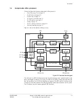
Figure 1-1
Processor block diagram ............................................................................................................ 1-4
Figure 1-2
Processor Fetch and Decode pipeline stages .......................................................................... 1-17
Figure 1-3
Cortex-R4 Issue and Execution pipeline stages ....................................................................... 1-17
Figure 1-4
Cortex-R4F Issue and Execution pipeline stages ..................................................................... 1-18
Figure 2-1
Byte-invariant big-endian (BE-8) format ...................................................................................... 2-6
Figure 2-2
Little-endian format ..................................................................................................................... 2-6
Figure 2-3
Register organization .................................................................................................................. 2-9
Figure 2-4
Program status register ............................................................................................................. 2-10
Figure 2-5
Interrupt entry sequence ........................................................................................................... 2-21
Figure 3-1
Power-on reset ............................................................................................................................ 3-7
Figure 3-2
AXI interface clocking ................................................................................................................. 3-9
Figure 4-1
System control and configuration registers ................................................................................. 4-4
Figure 4-2
MPU control and configuration registers ..................................................................................... 4-5
Figure 4-3
Cache control and configuration registers .................................................................................. 4-6
Figure 4-4
TCM control and configuration registers ..................................................................................... 4-6
Figure 4-5
System performance monitor registers ....................................................................................... 4-7
Figure 4-6
System validation registers ......................................................................................................... 4-7
Figure 4-7
Main ID Register format ............................................................................................................ 4-14
Figure 4-8
Cache Type Register format ..................................................................................................... 4-15
Figure 4-9
TCM Type Register format ........................................................................................................ 4-16
Figure 4-10
MPU Type Register format ....................................................................................................... 4-17
Figure 4-11
Multiprocessor ID Register format ............................................................................................ 4-18
Figure 4-12
Processor Feature Register 0 format ........................................................................................ 4-18
Figure 4-13
Processor Feature Register 1 format ........................................................................................ 4-19
Figure 4-14
Debug Feature Register 0 format ............................................................................................. 4-20
Figure 4-15
Memory Model Feature Register 0 format ................................................................................ 4-22


