


clears stored charges out of the switching transistors allowing a rapid turn off. Zener diode D13 lim-
its the voltage across C24 and C25 to 10 Volts under unusual conditions. The charge stored in
these capacitors is used to provide a large base current spike on subsequent turn on of the switch-
ing transistors which minimizes the turn on time.
When the main switch turns off, the flyback voltage of power transformer T7 is clamped by diode
D31 or the integral diode of Q19 and capacitor C29. Capacitor C30 and resistor R50 form a damper
to control oscillation of the voltage across C29 with the magnetizing inductance of T7. Transformer
T7 is demagnetized by reversing the current through C29 by the auxiliary switch MOSFET Q19
through diode D25 if used. The circuitry consisting of resistors R46, R47, R55, R53, diode D24 and
transistor Q18 initiate the turn on of Q19 when its drain to source voltage is less than approximately
80 volts. Q19 is turned off prior to turn on of the main switch via a pulse through T5 which turns on
Q20 via diode D29. Resistors R48 and R49 keep Q20 on, thus Q19 is off when it’s drain to source
voltage is in excess of 80 volts.
Components C32, C33, D32, L4, D26, D27, R57, C35 form a loss-less snubber which reduces the
switch voltage rise time to minimize the turn off loss of the transistor switch. The leakage induc-
tance of T7 is sufficient to limit the turn on loss. Zener diodes string D14-17 protects the transistor
switch from excessive voltages under rare transient conditions.
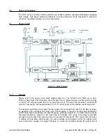
7.1.4
Output Circuit
The output secondary current of power transformer T7 passes through the forward half of D47 and
inductor L5 to the load when the main switch is on. When the main switch is off this load current
passes through the flyback half of D47 and not through the secondary of T7. Components C51,
C52 and R82-R96 form snubbers to control the rate of change of voltage of D47. Components
D49-D52, C54, C55 and R100 form a clamping network to limit the turn off spike voltages of D47 to
a safe level. Inductors L5 and L7 and capacitors C56, (C65) and C66 form a two-stage LC filter to
average the pulse train voltage at the input side of L5 to the desired DC output with a few mV of
ripple. Components C53, C63, C64 and L6 form a common mode filter to control the output com-
mon mode noise. Resistor R99 and R125 bleed the output and output to ground voltage respec-
tively for safety reasons.
7.1.5
Voltage and Current Sensing Circuitry
The output current is sensed across the 50 mV shunt resistor R126 by differential amplifiers U9 and
U10 which scale up the current representation to 5 volts at full output current. U9 provides output
current information for the current error amplifier and U10 for the front power circuitry. Differential
amplifier U8/B senses the output voltage via a voltage divider consisting of resistor networks R132
and R133. Either the local or remote output voltage is sensed as selected via analog switch U11 as
commanded by the front panel circuitry through Q27. Local sensing is also selected if the output cir-
cuit breaker is open via E42 or Q28 and Q26 or via E46-E47 for the negative output ground units.
7.1.6
Error Amplifiers
Operational amplifier U7/A is an error amplifier which regulates the flyback voltage of T7 under un-
usual conditions to protect the switching transistors and the output diode. A representation of the
flyback voltage is developed across capacitor C57 via winding E33-34 of T7, diode D53 and resistor
R101. This voltage is sensed by U7/A by resistors R106 and R107 and compared to a -5 volt refer-
ence developed across zener diode D35. Components C74, R71 and R112 provide frequency com-
pensation for the flyback regulating control loop. Diodes D37 and D38 keep U7/A in its “active” re-
gion when not regulating.
Current error amplifier U7/B compares the output current representation provided by U9 to the refer-
ence provided by the front panel circuitry. Resistor R114 and capacitor C60 provide noise filtering of
ARGUS TECHNOLOGIES
Document #010-002-C0 Rev. H Page 23
Summary of Contents for RST 48/30
Page 1: ...RST 48 30 Switched Mode Rectifier Eliminator 010 006 B0 ...
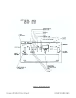
Page 24: ...Document 010 002 C0 Rev H Page 14 ARGUS TECHNOLOGIES Figure 3 Front Panel Layout ...
Page 52: ......
Page 53: ......
Page 63: ......
Page 75: ......


