EVAL-ADIN1110EBZ User Guide
Preliminary UG-XXXX
Rev. PrA | Page 11 of 23
LAYOUT GUIDELINES
BOARD STACKUP
The EVAL-ADIN1110EBZ consists of a 4-layer PCB: the top
layer, Layer 2, Layer 3, and the bottom layer. All layers have a
copper pour, with an extra keep-out area along the left-hand-
side of the board close to the Earth trace.
GROUND PLANES
The top and bottom layers of the EVAL-ADIN1110EBZ mainly
carry signal and routing signals from the ADIN1110. The two
inner layers are used for ground planes. Layer 2 is a full ground
plane. Layer 3 also has a ground plane but is also used to track
the power signals. Although the ADIN1110 is a mixed signal
device, it only has one type of ground return, GND.
POWER SUPPLY DECOUPLING
From a PCB layout point of view, it is important to locate the
decoupling capacitors as close as possible to the power supply
and GND pins to minimize the inductance.
SPI INTERFACE
When routing the SPI interface traces, avoid crossover of the
signals where possible. Stubs should be avoided on all signal
traces. It is recommended to route traces on the same layer.
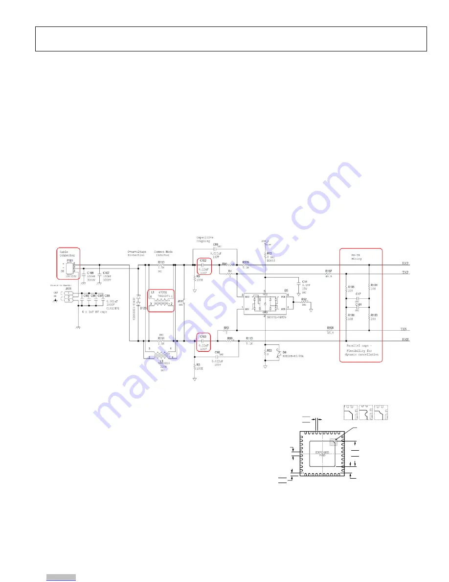
MDI INTERFACE
Traces running from the RXP/N and TXP/N pins of the
ADIN1110 to the external hybrid circuit (R103-R106, C17,
C101) must be, where possible, on the same side of the EVAL-
ADIN1110EBZ and kept as short as possible. The same
recommendations apply for traces running through the C102
and C104 series capacitors to the common mode choke and
onwards to the cable connector (P101) – see Figure 17.
Impedance must be kept constant throughout. Trace lengths
must be kept equal where possible and any right angles on these
traces must be avoided (use curves or 45° angles in the traces).
Stubs must be avoided on all signal traces.
Figure 17. MDI Interface Connections.
THERMAL CONSIDERATIONS
The ADIN1110 is packaged in an LFCSP package. This package
is designed with an exposed paddle which must be soldered to
the PCB for mechanical and thermal reasons. The exposed
paddle acts to conduct heat away from the package and into the
PCB. By incorporating an array of thermal vias in the PCB thermal
paddle, heat is dissipated more effectively into the inner metal
layers of the PCB. When designing the PCB layout for
optimum thermal performance, use a 4 mm × 4 mm array of
vias under the paddle.
3.60
3.50 SQ
3.40
BOTTOM VIEW
0.45
0.40
0.35
0.30
0.25
0.20
0.20 MIN
0.50
BSC
40
1
11
10
20
21
30
31
PI N 1
IN D I C AT O R AR E A OP T IO N S
(SEE DETAIL A)
DETAIL A
(JEDEC 95)
Figure 18. LFCSP Simplified Package Drawing
Downloaded from
Downloaded from
Downloaded from
Downloaded from
Downloaded from
Downloaded from
Downloaded from
Downloaded from
Downloaded from
Downloaded from
Downloaded from


