AD9854
Rev. E | Page 36 of 52
GENERAL OPERATION OF THE SERIAL INTERFACE
There are two phases of a serial communication cycle with the
AD9854. Phase 1 is the instruction cycle, which is the writing of
an instruction byte into the AD9854 coincident with the first
eight SCLK rising edges. The instruction byte provides the
AD9854 serial port controller with information regarding the
data transfer cycle, which is Phase 2 of the communication
cycle. The Phase 1 instruction byte defines whether the
upcoming data transfer is a read or write and the register
address to be acted upon.
The first eight SCLK rising edges of each communication cycle
are used to write the instruction byte into the AD9854. The
remaining SCLK edges are for Phase 2 of the communication
cycle. Phase 2 is the actual data transfer between the AD9854
and the system controller. The number of data bytes transferred
in Phase 2 of the communication cycle is a function of the
register address. (Table 10 describes how many bytes must be
transferred.) The AD9854 internal serial I/O controller expects
every byte of the register being accessed to be transferred.
Therefore, the user should write between I/O update clocks.
At the completion of a communication cycle, the AD9854 serial
port controller expects the subsequent eight rising SCLK edges
to be the instruction byte of the next communication cycle. In
addition, an active high input on the IO RESET pin immediately
terminates the current communication cycle. After IO RESET
returns low, the AD9854 serial port controller requires the
subsequent eight rising SCLK edges to be the instruction byte
of the next communication cycle.
All data input to the AD9854 is registered on the rising edge of
SCLK, and all data is driven out of the AD9854 on the falling
edge of SCLK.
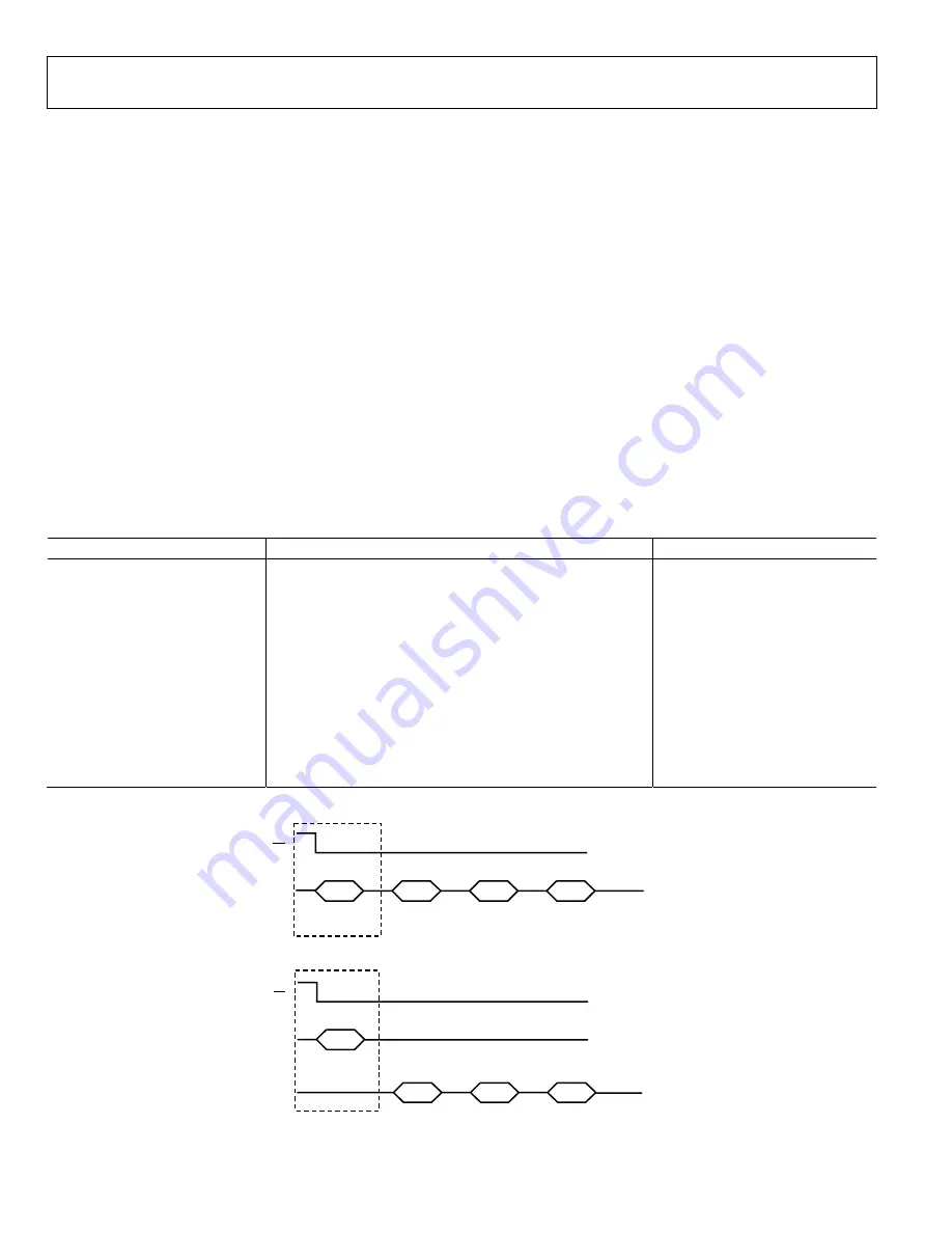
Figure 54 and Figure 55 show the general operation of the
AD9854 serial port.
Table 10. Register Address vs. Data Bytes Transferred
Serial Register Address
Register Name
Number of Bytes Transferred
0
Phase Offset Tuning Word Register 1
2
1
Phase Offset Tuning Word Register 2
2
2 Frequency
Tuning
Word
1
6
3 Frequency
Tuning
Word
2
6
4
Delta frequency register
6
5
Update clock rate register
4
6
Ramp rate clock register
3
7 Control
register
4
8
I path digital multiplier register
2
9
Q path digital multiplier register
2
A
Shaped on/off keying ramp rate register
1
B
Q DAC register
2
INSTRUCTION
CYCLE
DATA TRANSFER
INSTRUCTION
BYTE
DATA BYTE 1
DATA BYTE 2
DATA BYTE 3
SDIO
CS
006
36-
05
4
Figure 54. Using SDIO as a Read/Write Transfer
INSTRUCTION
CYCLE
DATA TRANSFER
INSTRUCTION
BYTE
SDIO
DATA TRANSFER
DATA BYTE 1
DATA BYTE 2
DATA BYTE 3
SDO
CS
006
36-
055
Figure 55. Using SDIO as an Input and SDO as an Output


