background image

AD9854 


Rev. E | Page 30 of 52 

12-BIT DIGITAL

MULTIPLIER

12

12

(BYPASS MULTIPLIER)

OSK EN = 0

OSK EN = 1

OSK EN = 0

OSK EN = 1

12

12

DIGITAL

SIGNAL IN

USER-PROGRAMMABLE

12-BIT Q CHANNEL

MULTIPLIER

OUTPUT SHAPED

KEYING Q MULTIPLIER

REGISTER

12

OSK INT = 0

OSK INT = 0

1

8-BIT RAMP

RATE

COUNTER

SYSTEM

CLOCK

ON/OFF OUTPUT SHAPED

KEYING PIN

SINE DAC

12-BIT

UP/DOWN

COUNTER

DDS DIGITAL

OUTPUT

0

063

6-

0

50


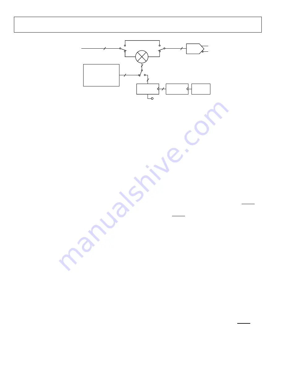
Figure 50. Block Diagram of Q DAC Pathway of the Digital Multiplier Section Responsible for the Output Shaped Keying Function 


The two fixed elements of the transition time are the period of 
the system clock (which drives the ramp rate counter) and the 
number of amplitude steps (4096). For example, if the system 
clock of the AD9854 is 100 MHz (10 ns period) and the ramp 
rate counter is programmed for a minimum count of 3, the 
transition takes two system clock periods (one rising edge loads 
the countdown value, and the next edge decrements the counter 
from 3 to 2). If the countdown value is less than 3, the ramp rate 
counter stalls and therefore produces a constant scaling value to 
the digital multipliers. This stall condition may have an application 
for the user.  

The relationship of the 8-bit countdown value to the time 
between output pulses is given as 

(

N

 + 1) × 

System Clock Period


where 

N

 is the 8-bit countdown value.  

It takes 4096 of these pulses to advance the 12-bit up-counter 
from zero scale to full scale. Therefore, the minimum output 
shaped keying ramp time for a 100 MHz system clock is  

4096 × 4 × 10 ns ≈ 164 μs 

The maximum ramp time is  

4096 × 256 × 10 ns ≈ 10.5 ms 

Finally, changing the logic state of Pin 30, output shaped keying 
automatically performs the programmed output envelope functions 
when OSK INT is high. A logic high on Pin 30 causes the outputs 
to linearly ramp up to full-scale amplitude and to hold until the 
logic level is changed to low, causing the outputs to ramp down 
to zero scale. 

I AND Q DACS 

The sine and cosine outputs of the DDS drive the Q and I DACs, 
respectively (300 MSPS maximum). The maximum amplitudes 
of these output are set by the DAC R

SET

 resistor at Pin 56. These 

are current-output DACs with a full-scale maximum output of 
20 mA; however, a nominal 10 mA output current provides the 
best spurious-free dynamic range (SFDR) performance. The value 

of R

SET

 is 39.93/I

OUT

, where I

OUT

 is expressed in amps. DAC output 

compliance specifications limit the maximum voltage developed 
at the outputs to −0.5 V to +1 V. Voltages developed beyond this 
limitation cause excessive DAC distortion and possibly permanent 
damage. The user must choose a proper load impedance to limit 
the output voltage swing to the compliance limits. Both DAC 
outputs should be terminated equally for best SFDR, especially 
at higher output frequencies, where harmonic distortion errors 
are more prominent. 

Both DACs are preceded by inverse sin(x)/x filters (also called 
inverse sinc filters) that precompensate for DAC output amplitude 
variations over frequency to achieve flat amplitude response from 
dc to Nyquist. Both DACs can be powered down when not needed 
by setting the DAC PD bit high (Address 1D hex of the control 
register). I DAC outputs are designated as IOUT1 and IOUT1, 
Pin 48 and Pin 49, respectively. Q DAC outputs are designated 
as IOUT2 and IOUT2, Pin 52 and Pin 51, respectively. 

CONTROL DAC 

The 12-bit Q DAC can be reconfigured to perform as a control 
or auxiliary DAC. The control DAC output can provide dc 
control levels to external circuitry, generate ac signals, or enable 
duty cycle control of the on-board comparator. When the SRC 
Q DAC bit in the control register (Parallel Address 1F hex) is  
set high, the Q DAC inputs are switched from internal 12-bit 
Q data source (default setting) to external 12-bit, twos complement 
data supplied by the user. Data is channeled through the serial 
or parallel interface to the 12-bit Q DAC register (Address 26 hex 
and Address 27 hex) at a maximum data rate of 100 MHz. This 
DAC is clocked at the system clock, 300 MSPS (maximum), and 
has the same maximum output current capability as that of the I 
DAC. The single R

SET

 resistor on the AD9854 sets the full-scale 

output current for both DACs. When not needed, the control 
DAC can be separately powered down to conserve power by 
setting the Q DAC power-down bit high (Address 1D hex). 
Control DAC outputs are designated as IOUT2 and IOUT2,  
Pin 52 and Pin 51, respectively. 

Summary of Contents for AD9854

Page 1: ...rrection Simplified control interfaces 10 MHz serial 2 or 3 wire SPI compatible 100 MHz parallel 8 bit programming 3 3 V single supply Multiple power down functions Single ended or differential input...

Page 2: ...rol DAC 30 Inverse Sinc Function 31 REFCLK Multiplier 31 Programming the AD9854 32 MASTER RESET 32 Parallel I O Operation 34 Serial Port I O Operation 34 General Operation of the Serial Interface 36 I...

Page 3: ...le Tone Mode 000 Section 17 Changes to Ramped FSK Mode 010 Section 18 Changes to Basic FM Chirp Programming Steps Section 23 Changes to Figure 50 27 Changes to Evaluation Board Operating Instructions...

Page 4: ...used for phase changes The 12 bit I and Q DACs coupled with the innovative DDS architecture provide excellent wideband and narrow band output SFDR The Q DAC can also be configured as a user programma...

Page 5: ...C IV 1 1 V DAC STATIC OUTPUT CHARACTERISTICS Output Update Speed Full I 300 200 MSPS Resolution 25 C IV 12 12 Bits I and Q Full Scale Output Current 25 C IV 5 10 20 5 10 20 mA I and Q DAC DC Gain Imb...

Page 6: ...C IV 10 10 SYSCLK cycles COMPARATOR INPUT CHARACTERISTICS Input Capacitance 25 C V 3 3 pF Input Resistance 25 C IV 500 500 k Input Current 25 C I 1 5 1 5 A Hysteresis 25 C IV 10 20 10 20 mV p p COMPA...

Page 7: ...et square or sine wave centered at one half the applied VDD or a 3 V TTL level pulse input 2 An internal 400 mV p p differential voltage swing equates to 200 mV p p applied to both REFCLK input pins 3...

Page 8: ...EDEC test board 3 Values of JA are provided for package comparison and PCB design considerations 4 Per JEDEC JESD51 6 heat sink soldered to PCB 5 Airflow increases heat dissipation effectively reducin...

Page 9: ...7 28 72 75 to 78 DGND Connections for the Digital Circuitry Ground Return Same potential as AGND 13 35 57 58 63 NC No Internal Connection 14 to 16 A5 to A3 Parallel Address Inputs for Program Register...

Page 10: ...ternal high speed comparator 43 VINN Voltage Input Negative The inverting input of the internal high speed comparator 48 IOUT1 Unipolar Current Output of I or the Cosine DAC Refer to Figure 3 49 IOUT1...

Page 11: ...THE OUTPUT VOLTAGE COMPLIANCE RATING COMPARATOR OUT AVDD DVDD DIGITAL IN AVOID OVERDRIVING DIGITAL INPUTS FORWARD BIASING ESD DIODES MAY COUPLE DIGITAL NOISE ONTO POWER PINS A DAC OUTPUTS B COMPARATO...

Page 12: ...0636 004 Figure 4 Wideband SFDR 19 1 MHz 0 START 0Hz 10 20 30 40 50 60 70 80 90 100 15MHz STOP 150MHz 00636 005 Figure 5 Wideband SFDR 39 1 MHz 0 START 0Hz 10 20 30 40 50 60 70 80 90 100 15MHz STOP 15...

Page 13: ...d SFDR 39 1 MHz 1 MHz BW 300 MHz REFCLK with REFCLK Multiplier Bypassed 0 CENTER 39 1MHz 10 20 30 40 50 60 70 80 90 100 5kHz SPAN 50kHz 00636 011 Figure 11 Narrow Band SFDR 39 1 MHz 50 kHz BW 300 MHz...

Page 14: ...lier 10 100 110 150 120 130 140 160 170 PHASE NOISE dBc Hz AOUT 80MHz AOUT 5MHz FREQUENCY Hz 10 1M 100 100k 10k 1k 00636 018 Figure 18 Residual Phase Noise 300 MHz REFCLK with REFCLK Multiplier Bypass...

Page 15: ...itter 40 MHz AOUT 300 MHz RFCLK with REFCLK Multiplier Bypassed CH1 500mV M 500ps CH1 980mV REF1 RISE 1 174ns C1 FALL 1 286ns 00636 023 Figure 23 Comparator Rise Fall Times FREQUENCY MHz 1200 0 AMPLIT...

Page 16: ...8 10 BIT ADC DIGITAL DEMODULATOR Rx BASEBAND DIGITAL DATA OUT 8 8 I Q MIXER AND LOW PASS FILTER VCA ADC ENCODE ADC CLOCK FREQUENCY LOCKED TO Tx CHIP SYMBOL PN RATE REFERENCE CLOCK 48 CHIP SYMBOL PN RA...

Page 17: ...0 8 TO 2 5GHz AD9854 QUADRATURE DDS DDS LO LO DDS LO 36dB TYPICAL SSB REJECTION 50 VOUT AD8346 QUADRATURE MODULATOR 90 COSINE DC TO 70MHz SINE DC TO 70MHz LO LO 0 00636 031 NOTES 1 FLIP DDS QUADRATURE...

Page 18: ...I DAC 1 2 Q DAC OR CONTROL DAC LOW PASS FILTER LOW PASS FILTER 00636 034 NOTES 1 IOUT APPROX 20mA MAX WHEN RSET 2k 2 SWITCH POSITION 1 PROVIDES COMPLEMENTARY SINUSOIDAL SIGNALS TO THE COMPARATOR TO PR...

Page 19: ...1 1 Chirp 1 0 0 BPSK In each mode some functions may be prohibited Table 6 lists the functions and their availability for each mode Single Tone Mode 000 This is the default mode when the MASTER RESET...

Page 20: ...ated via the 8 bit parallel programming port at a 100 MHz parallel byte rate or at a 10 MHz serial rate Incorporating this attribute permits FM AM PM FSK PSK and ASK operation in single tone mode Unra...

Page 21: ...raditional FSK Mode I O UD CLK F1 F2 0 FREQUENCY MODE TW1 TW2 010 RAMPED FSK F1 F2 000 DEFAULT 0 0 REQUIRES A POSITIVE TWOS COMPLEMENTVALUE RAMP RATE DFW FSK DATA PIN 29 00636 037 Figure 37 Ramped FSK...

Page 22: ...ter is activated when a logic level change occurs on the FSK input Pin 29 This counter is run at the system clock rate 300 MHz maximum The time period between each output pulse is given as N 1 System...

Page 23: ...dwell times at every frequency Use this function to automatically sweep between any two frequencies from dc to Nyquist In the ramped FSK mode with the triangle bit set high an automatic frequency swe...

Page 24: ...trol bit Register Address 1F hex is available to clear both the frequency accumulator ACC1 and the phase accumulator ACC2 When this bit is set high the output of the phase accumulator results in 0 Hz...

Page 25: ...0 Hz When the CLR ACC1 bit Register Address 1F hex is set high the 48 bit frequency accumulator ACC1 output is cleared with a retriggerable one shot pulse of one system clock duration The 48 bit delt...

Page 26: ...F1 000 DEFAULT 0 RAMP RATE RAMP RATE 011 CHIRP DELTA FREQUENCY WORD CLR ACC1 00636 045 Figure 45 Effect of CLR ACC1 in FM Chirp Mode CLR ACC2 F1 0 FREQUENCY MODE TW1 DPW 000 DEFAULT 0 RAMP RATE 011 CH...

Page 27: ...ange between dc and Nyquist Unless terminated by the user the chirp continues until power is removed When the chirp destination frequency is reached the user can choose any of the following actions St...

Page 28: ...solution to achieve the proper frequency range BPSK Mode 100 Binary biphase or bipolar phase shift keying is a means to rapidly select between two preprogrammed 14 bit output phase offsets that equall...

Page 29: ...ansferring This is an effect of the minimum high pulse time when I O UD CLK functions as an output ON OFF OUTPUT SHAPED KEYING OSK The on off OSK feature allows the user to control the amplitude vs ti...

Page 30: ...in 56 These are current output DACs with a full scale maximum output of 20 mA however a nominal 10 mA output current provides the best spurious free dynamic range SFDR performance The value of RSET is...

Page 31: ...in 61 provides the connection for the external zero compensation network of the PLL loop filter The zero compensation network consists of a 1 3 k resistor in series with a 0 01 F capacitor The other s...

Page 32: ...rt after the contents of the buffer memory are transferred to the register banks This transfer of information occurs synchronously to the system clock in one of two ways Internally at a rate programma...

Page 33: ...lta frequency word 23 16 00 14 Delta frequency word 15 8 00 15 Delta frequency word 7 0 00 16 5 Update clock 31 24 00 17 Update clock 23 16 00 18 Update clock 15 8 00 19 Update clock 7 0 40 1A 6 Ramp...

Page 34: ...and can be configured as a single pin I O SDIO or two unidirectional pins for input and output SDIO SDO Data transfers are supported in MSB or the LSB first format for up to 10 MHz When configured fo...

Page 35: ...36 052 Figure 52 Parallel Port Read Timing Diagram D 7 0 D1 D2 D3 SPECIFICATION VALUE DESCRIPTION tASU tDSU tADH tDHD 8 0ns 3 0ns ADDRESS SETUP TIME TO WR SIGNAL ACTIVE DATA SETUP TIME TO WR SIGNAL AC...

Page 36: ...controller expects the subsequent eight rising SCLK edges to be the instruction byte of the next communication cycle In addition an active high input on the IO RESET pin immediately terminates the cu...

Page 37: ...yte NOTES ON SERIAL PORT OPERATION The AD9854 serial port configuration bits reside in Bit 1 and Bit 0 of Register Address 20 hex It is important to note that the configuration changes immediately upo...

Page 38: ...the clocks are forced to dc effectively powering down the digital section In this state the PLL still accepts the REFCLK signal and continues to output the higher frequency CR 23 is reserved Write to...

Page 39: ...n is configured as an input CR 7 is reserved Write to 0 CR 6 is the inverse sinc filter bypass bit When this bit is set the data from the DDS block goes directly to the output shaped keying logic and...

Page 40: ...convenience can be the ground plane Sockets for either package style of the device are not recommended JUNCTION TEMPERATURE CONSIDERATIONS The power dissipation PDISS of the AD9854 in a given applica...

Page 41: ...ed operating temperature for the AD9854 in a given application Subtract this value from 150 C which is the maximum junction temperature allowed for the AD9854 For the extended industrial temperature r...

Page 42: ...Windows 95 Windows 98 Windows 2000 Windows NT and Windows XP Connect a printer cable from the PC to the AD9854 evaluation board printer port connector labeled J11 Hardware Preparation Use the schemat...

Page 43: ...Q signals appear as nearly pure sine waves and 90 out of phase with each other These filters are designed with the assumption that the system clock speed is at or near its maximum speed 300 MHz If the...

Page 44: ...al entries such as frequency and phase infor mation require pressing Enter to register the information For example if a new frequency is input but does not take effect when Load is clicked the user pr...

Page 45: ...06CG120J9B200 10 2 C34 C43 Capacitor 1206 1206 8 2 pF 50 V NPO 0 5 pF Yageo Corporation CC1206DRNPO9BN8R2 11 9 J1 J2 J3 J4 J5 J6 J7 J25 J26 SMB STR PC MNT N A N A Emerson Johnson 131 3701 261 12 1 J10...

Page 46: ...5552742 1 31 6 W1 W2 W3 W4 W8 W17 3 pin header SIP 3P N A N A Samtec Inc TSW 103 07 S S 32 10 W6 W7 W9 W10 W11 W12 W13 W14 W15 W16 2 pin header SIP 2P N A N A Samtec Inc TSW 102 07 S S 33 6 W1 W2 W3 W...

Page 47: ...F C27 0 1 F C8 0 1 F C44 0 1 F GND DVDD J10 1 2 3 4 5 6 7 8 9 10 11 12 13 14 15 16 17 18 19 20 21 22 23 24 25 26 27 28 29 30 31 32 33 34 35 36 37 38 39 40 ADR5 ADR4 ADR3 ADR2 ADR1 ADR0 UDCLK WR RD PMO...

Page 48: ...CC 20 RESET UDCLK PMODE ORAMP FDATA U4 74HC125D GND 1G 1A 1Y 2G 2A 2Y VCC 4G 4A 4Y 3G 3A 3Y U2 GND 1 2 3 4 5 6 7 13 12 11 10 9 8 14 VCC VCC U10 W11 ADDR1 ADDR0 W14 W12 W13 W9 VCC R18 10k GND W15 VCC R...

Page 49: ...AD9854 Rev E Page 49 of 52 00636 070 Figure 66 Assembly Drawing 00636 071 Figure 67 Top Routing Layer Layer 1...

Page 50: ...AD9854 Rev E Page 50 of 52 00636 072 Figure 68 Power Plane Layer Layer 3 00636 073 Figure 69 Ground Plane Layer Layer 2...

Page 51: ...AD9854 Rev E Page 51 of 52 00636 074 Figure 70 Bottom Routing Layer Layer 4...

Page 52: ...ITY VIEW A ROTATED 90 CCW SEATING PLANE 7 3 5 0 61 60 1 80 20 41 21 40 VIEW A 1 60 MAX 0 75 0 60 0 45 16 20 16 00 SQ 15 80 14 20 14 00 SQ 13 80 0 65 BSC LEAD PITCH 0 38 0 32 0 22 TOP VIEW PINS DOWN PI...

Reviews: