


Quick Start Guide
AD9789-EBZ
Rev. A | Page 6 of 8
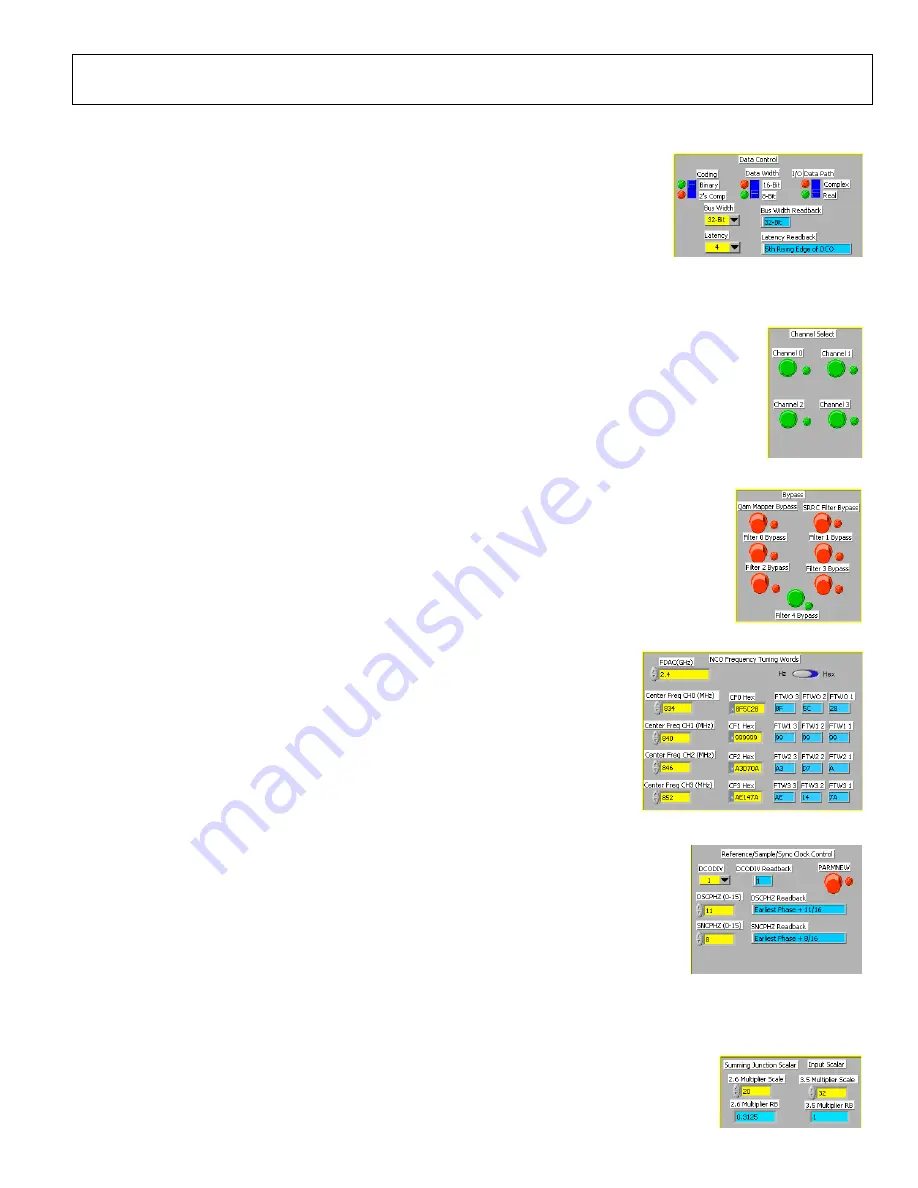
Data Control
These bits control how the data is interpreted by the AD9789. The Coding switch selects between
Binary (unsigned) and 2’s Comp (signed, 2’s compliment format). Both options are valid for this
evaluation system. Ensure that the vectors used are in the correct format.
The Bus Width, Data With, and Data Path switches control how the data is sent over the bus.
Regardless of what these are set to, the DPGDownloader settings must match for proper data transfer.
The Latency switch controls when the AD9789 beings sampling data. For the DPG2, this should be
left at 4, for LVDS bus mode, or 5 for CMOS bus mode.
Channel Select
The four switches in this section control which of the four data channels are enabled. If the CHANPRI bit is high (see
Interface Control
section), all four channels in DPGDownloader should be enabled, regardless of the setting of these
switches. However, if CHANRPI is low, then the channels in DPGDownloader should be enable or disabled in
accordance with these switches.
In QDUC Mode, all channels will get identical data. It is common in this case to turn off all but one channel.
Bypass Controls
The switches in this section determine which of the functional blocks in the data path are enabled. Red indicates
that the block is enabled (and thus not bypassed), while green indicates the block is disabled (bypassed). Each of
the filters (the SRRC and Filter 0 through Filter 4) will drop the frequency of the frame sync by two (and thus the
effective sample rate). They will not affect the DCO frequency (which is displayed in DPGDownloader). The
QAM Mapper must be disabled in QDUC Mode.
Numerically Controlled Oscillator (NCO) Frequency Controls
The controls in this section affect where the four carriers will be placed, using the internal
modulators. First, enter the frequency of the input clock in the FDAC box. Then, enter the
desired carrier frequencies. Note that all four carriers must appear in ascending order, 6MHz
apart. For example, in Figure 15, the first carrier is at 834MHz. The next carrier is 6MHz above
this, at 840MHz. The next carriers fall at 846MHz and 852MHz, each 6MHz above the previous
carrier. The SPI controller software will automatically calculate the required register value in hex
for the desired frequency. To input the hex value directly, move the horizontal switch to
Hex
.
Reference/Sample/Sync Clock Control
The DCODIV control determines the frequency of the Data Clock Out (DCO) clock. This clock
is provided to the DPG2, and is used as the data sample clock. The DCO frequency will always be 1/16
th
of the input clock, in addition to whatever division is selected in this section.
The DSCPHZ and SNCPHZ controls affect when the AD9789 samples the data on the bus. Refer to the
datasheet for detailed information on the proper setting of these options. The default values of 11 and 8
are correct for using the AD9789-EBZ with the DPG2 with a clock in the 2GHz range.
After any of the options in this section are changed, the PARMNEW bit must be cycled. Enabled it
(green), run the SPI controller to apply it, and then disable it (red) and run the SPI controller again.
Summing Junction Scalar and Input Scalar Controls
These options will not affect the evaluation system per-se. However, if these are set too high, the AD9789 will
saturate internally, leading to a very poor output spectrum. Refer to the datasheet for recommended values.
The
Interrupt Request Controls
contain a saturation counter to aid in determining if saturation has occurred. If
Figure 12
Figure 13
Figure 14
Figure 15
Figure 16
Figure 17


