Analog Devices AD9789-EBZ Quick Start Manual Download Page 3

Quick Start Guide 

AD9789-EBZ 


Rev. A | Page 3 of 8 

Figure 5


Internal QAM Test 

In  this  example,  the  AD9789  is  configured  to  generate  a  QAM  vector  internally  by  using  the  internal  pseudo-random  number  (PRN) 
generator in conjunction with the on-chip QAM encoder. This allows the user to measure the AC performance of a QAM signal at the 
DAC output without needing an external data source. The steps that follow show the user how to enable the internal PRN generator and 
setup  each  channel  of  the  data  path  to  map  the  PRN  to  256QAM,  shape  and  interpolate  the  QAM  carrier  such  that  it  is  DOCSIS 
compliant and modulate each channel to 834MHz, 840MHz, 846MHz, and 852MHz respectively (Fdac=2.29376GHz). 

Install the software as described in the 

Software

 section, and connect all the required cables as described in the 

Hardware Setup

 section. 

Turn  on  the  power  supply.  The  current  should  be  approximately  200mA.  For  this  setup,  the  clock  source  should  be  set  to  generate  a 
2.29376GHz tone at 2dBm. Jumpers JP9 and JP10 should be set to their LVDS position (towards the DPG2 connector). 

Open the AD9789 PRN software (Start > Programs > Analog Devices > AD9789-EBZ > AD9789 PRN). Click Run, and wait for the status 
indicator to become bright green. Next, open the AD9789 SPI application (Start > Programs > Analog Devices > AD9789-EBZ > AD9789 
SPI).  Click  the  Load  button,  and  then  click  the  Run  button  ( ).  When  prompted  for  a  file  to  load,  select 

AD9789_SPISettings_Int_QAM.txt

.  Once  that  run  has  completed,  click  the  Load  button  again  to  de-select  it.  Enable  the  PARMNEW 

button, and click Run again. De-select PARMNEW after the run has completed. 

Also, ensure that the FREQNEW control bit is set.  This bit needs to be set for any changes made to the center frequency of the BPF and 
the rate converter (P/Q) to take effect.  If the FREQNEW is set properly, the read back indicators for the rate converter and BPF will be 
updated  to  the  correct  values  upon  the  second  run  of  the  SPI  program.  Note  that  FREQNEW  is  a  self-clearing  bit  and  can  therefore 
always be set high. 

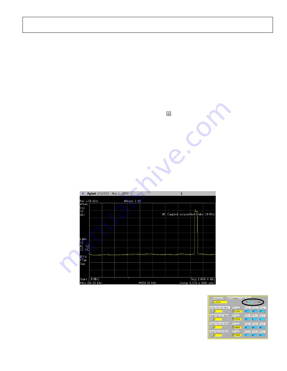
Expected DAC Performance 

For the setup described in above the expected DAC output spectral performance is illustrated in Figure 4. 


DAC  Settings:  f

DAC 

=  2.29376GHz,  f

C0 

=  834MHz,  f

C1 

=  840MHz,  f

C2 

=  846MHz,  f

C3 

=  852MHz,  f

BPF 

=  843MHz,  QAM  Mapper,  SRRC, 

Filters1-4 enabled 


Figure 4 

The center frequencies, QAM Mapper modes, # of carriers, etc. can be varied for an assortment of 
AC performance testing.   


Take  note of  the Hz  or Hex  slide control  in  Figure  5.   Once a SPI configuration  file  is  loaded  this 
slide control  will  be  set  to Hex, meaning  that  center  frequencies  of  the  channels are  controlled  by 
entering the Frequency Tuning Word (FTW) for each NCO.  The user can opt to change this control 
to Hz and control the center frequencies of the channels by inputting the desired frequency in MHz 
and the software will calculate the FTW. Note that for this calculation to be accurate, the user must 
also enter the DAC rate in GHz. 

Summary of Contents for AD9789-EBZ

Page 1: ... 2 DPG2 INTRODUCTION The AD9789 EBZ Evaluation Board connects to a DPG2 to allow for quick evaluation of the AD9789 Control of the SPI port in the AD9789 is available through USB with accompanying PC software The AD9789 EBZ allows evaluation of both CMOS and LVDS modes as well as numerous interface modes of the AD9789 The DPGDownloader software automatically formats the data sent to the DPG2 to ac...

Page 2: ...MOS position away from the DPG2 connector Open the AD9789 SPI application from your Start Menu Start Programs Analog Devices AD9789 EBZ AD9789 SPI In the lower left click the Load button it will stay depressed Press the Run button in the upper left A dialog will appear asking for the file to load Open AD9789_SPIsettings_Int_Sine_Wave txt located in the same directory as the SPI controller After th...

Page 3: ...n When prompted for a file to load select AD9789_SPISettings_Int_QAM txt Once that run has completed click the Load button again to de select it Enable the PARMNEW button and click Run again De select PARMNEW after the run has completed Also ensure that the FREQNEW control bit is set This bit needs to be set for any changes made to the center frequency of the BPF and the rate converter P Q to take...

Page 4: ...imately 1 0A Set the spectrum analyzer to center at 843MHz with a 24MHz span and 30kHz resolution bandwidth Four tones should now be visible at 834MHz 840MHz 846MHz and 852MHz Click on the PARMNEW button in the SPI controller It should turn red Click Run again The LOCK indicator in the upper left of the screen should now be green The part is now ready to receive data Open DPGDownloader on your PC ...

Page 5: ...he USB hardware unable to communicate with the AD9789 If these bits become set a hard reset power cycle will be required to restore their original settings Interrupt Request Controls These controls enable and disable the various interrupts available on the AD9789 These settings will not affect the evaluation system although the LOCK and LOCKLOST indicators are useful when debugging clock issues In...

Page 6: ...ency Controls The controls in this section affect where the four carriers will be placed using the internal modulators First enter the frequency of the input clock in the FDAC box Then enter the desired carrier frequencies Note that all four carriers must appear in ascending order 6MHz apart For example in Figure 15 the first carrier is at 834MHz The next carrier is 6MHz above this at 840MHz The n...

Page 7: ...of the count Rate Converter Controls The Rate Converter will affect the frequency of the Frame Sync signal If the rate converter ratio is too large certain modes that require many clock cycles may not be able to function The Center Frequency BPF should be set to center frequency of all active channels This will ensure that the band pass filter is centered on where the carriers are Figure 18 ...

Page 8: ...lication has finished writing to the AD9516 it can be closed Connect the clock source to S6 REF_CLK_IN and set it to generate a 95 573MHz clock with 0dBm amplitude This will generate a 2 29376GHz clock for the AD9789 This signal is also available at S10 S11 for debugging the AD9516 ELECTRICAL INTERFACE SELECTION The AD9789 EBZ is designed to allow evaluation of both the CMOS and LVDS modes of the ...

Reviews: