Analog Devices AD9789-EBZ Quick Start Manual Download Page 4

Quick Start Guide 

AD9789-EBZ 


Rev. A | Page 4 of 8 


Below are the recommended Sum Scale values for all QAM Mapper modes and channel counts. 

Sum Scale Value 

QAM  

Mode 

1 Channel 

2 Channel 

3 Channel 

4 Channel 

DVB 16-QAM 

48 

28 

22 

16 

DVB 32-QAM 

54 

34 

26 

20 

DVB 64-QAM 

54 

34 

26 

20 

DVB 128-QAM 

80 

50 

38 

30 

DVB 256-QAM 

54 

34 

26 

20 

DOCSIS 64-QAM 

54 

34 

26 

20 

DOCSIS 256-QAM 

54 

34 

26 

20 

                                                                                                   Table 1 


QAM Vector Playback with the DPG2 

Install the software as described in the 

Software

 section, and connect all the required cables as described in the 

Hardware Setup

 section. 

Turn on the power supply. The current should be approximately 200mA. Turn on the clock source, with a 2.4GHz tone at 2dBm. This 
setup will use the LVDS mode, so ensure that jumpers JP9 and JP10 are in their LVDS positions (towards the DPG2 connector). 

Open the AD9789 SPI application from your Start Menu (Start > Programs > Analog Devices > AD9789-EBZ > AD9789 SPI). If you have 
the SPI controller open from a previous setup, close and re-open it before continuing. Press the Run ( ) button in the upper left. The 
current  measured  by  the  power  supply  should  jump  to  approximately  1.0A.  Set  the  spectrum  analyzer  to  center  at  843MHz,  with  a 
24MHz span, and 30kHz resolution bandwidth. Four tones should now be visible, at 834MHz, 840MHz, 846MHz, and 852MHz. Click on 
the  PARMNEW  button  in  the SPI  controller.  It  should  turn  red.  Click  Run again. The LOCK  indicator in  the  upper  left  of  the  screen 
should now be green. 

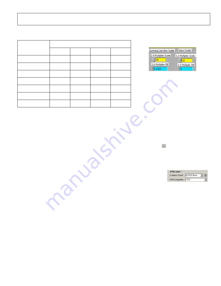
The part is now ready to receive data. Open DPGDownloader on your PC (Start > Programs > Analog 
Devices  >  DPG  >  DPGDownloader).  Under  the  Evaluation  Board  drop  down  list,  the  AD9789  should 
already be selected (if it is not, select it). For the Port Configuration, select LVDS. Once the configuration 
download is complete, it should be setup as shown in Figure 7. Now load in the included example vector 
of  random  data  by  clicking  Add  Data  File.  The  vector  can  be  found  in 

C:\Program  Files\Analog 

Devices\HSDAC\AD9789\Random Data.hex

 
Once the file has been processed by DPGDownloader, the software must be setup to match the settings in the AD9789. Select 32-Bit for 
the Bus Width, 8-bit for the Data Width, and Real for the Data Format. Select the check boxes next to each channel (4 in all). For the Real 
Data Vector in Channel 1, select 

Random Data.hex

 from the drop down list. Leave the other channels with 

None

 as the vector. Figure 8 

show the DPGDownloader software configured.  


Figure 7


Figure 6


Summary of Contents for AD9789-EBZ

Page 1: ... 2 DPG2 INTRODUCTION The AD9789 EBZ Evaluation Board connects to a DPG2 to allow for quick evaluation of the AD9789 Control of the SPI port in the AD9789 is available through USB with accompanying PC software The AD9789 EBZ allows evaluation of both CMOS and LVDS modes as well as numerous interface modes of the AD9789 The DPGDownloader software automatically formats the data sent to the DPG2 to ac...

Page 2: ...MOS position away from the DPG2 connector Open the AD9789 SPI application from your Start Menu Start Programs Analog Devices AD9789 EBZ AD9789 SPI In the lower left click the Load button it will stay depressed Press the Run button in the upper left A dialog will appear asking for the file to load Open AD9789_SPIsettings_Int_Sine_Wave txt located in the same directory as the SPI controller After th...

Page 3: ...n When prompted for a file to load select AD9789_SPISettings_Int_QAM txt Once that run has completed click the Load button again to de select it Enable the PARMNEW button and click Run again De select PARMNEW after the run has completed Also ensure that the FREQNEW control bit is set This bit needs to be set for any changes made to the center frequency of the BPF and the rate converter P Q to take...

Page 4: ...imately 1 0A Set the spectrum analyzer to center at 843MHz with a 24MHz span and 30kHz resolution bandwidth Four tones should now be visible at 834MHz 840MHz 846MHz and 852MHz Click on the PARMNEW button in the SPI controller It should turn red Click Run again The LOCK indicator in the upper left of the screen should now be green The part is now ready to receive data Open DPGDownloader on your PC ...

Page 5: ...he USB hardware unable to communicate with the AD9789 If these bits become set a hard reset power cycle will be required to restore their original settings Interrupt Request Controls These controls enable and disable the various interrupts available on the AD9789 These settings will not affect the evaluation system although the LOCK and LOCKLOST indicators are useful when debugging clock issues In...

Page 6: ...ency Controls The controls in this section affect where the four carriers will be placed using the internal modulators First enter the frequency of the input clock in the FDAC box Then enter the desired carrier frequencies Note that all four carriers must appear in ascending order 6MHz apart For example in Figure 15 the first carrier is at 834MHz The next carrier is 6MHz above this at 840MHz The n...

Page 7: ...of the count Rate Converter Controls The Rate Converter will affect the frequency of the Frame Sync signal If the rate converter ratio is too large certain modes that require many clock cycles may not be able to function The Center Frequency BPF should be set to center frequency of all active channels This will ensure that the band pass filter is centered on where the carriers are Figure 18 ...

Page 8: ...lication has finished writing to the AD9516 it can be closed Connect the clock source to S6 REF_CLK_IN and set it to generate a 95 573MHz clock with 0dBm amplitude This will generate a 2 29376GHz clock for the AD9789 This signal is also available at S10 S11 for debugging the AD9516 ELECTRICAL INTERFACE SELECTION The AD9789 EBZ is designed to allow evaluation of both the CMOS and LVDS modes of the ...

Reviews: