background image

ADM-PCIE-9V5 User Manual
 

when system resets and power cycles are not an option.

The Alpha Data System Monitor is also capable of reconfiguring the flash memory and reprograming the FPGA.

This provides a useful failsafe mechanism to re-program the FPGA even if it drops off the PCIe bus. The system

monitor can be accessed with avr2util over USB at the front panel and rear edge.

3.8.1.1 Building and Programming Configuration Images

Generate a bitfile with these constraints (see xapp1233):

set_property BITSTREAM.GENERAL.COMPRESS TRUE [ current_design ]

set_property BITSTREAM.CONFIG.EXTMASTERCCLK_EN {DIV-1} [current_design]

set_property BITSTREAM.CONFIG.SPI_32BIT_ADDR YES [current_design]

set_property BITSTREAM.CONFIG.SPI_BUSWIDTH 8 [current_design]

set_property BITSTREAM.CONFIG.SPI_FALL_EDGE YES [current_design]

set_property BITSTREAM.CONFIG.UNUSEDPIN {Pullnone} [current_design]

set_property CFGBVS GND [ current_design ]

set_property CONFIG_VOLTAGE 1.8 [ current_design ]

set_property BITSTREAM.CONFIG.OVERTEMPSHUTDOWN Enable [current_design]

Generate an MCS file with these properties (write_cfgmem):

-format MCS

-size 256

-interface SPIx8

-loadbit "up 0x0000000 <directory/to/file/filename.bit>" (0th location)

Program with vivado hardware manager with these settings (see xapp1233):

SPI part: mt25qu01g-spi-x1_x2_x4_x8

State of non-config mem I/O pins: Pull-none

3.8.2 Configuration via JTAG

A micro-USB AB Cable may be attached to the front panel or rear edge USB port. This permits the FPGA to be

reconfigured using the Xilinx Vivado Hardware Manager via the integrated Digilent JTAG converter box. The

device will be automatically recognized in Vivado Hardware Manager.

For more detailed instructions, please see “Using a Vivado Hardware Manager to Program an FPGA Device”

section of Xilinx UG908: https://www.xilinx.com/support/documentation/sw_manuals/xilinx2014_1/

ug908-vivado-programming-debugging.pdf

Page 19

Functional Description
ad-ug-1385_v1_0.pdf

Summary of Contents for ADM-PCIE-9V5

Page 1: ...ADM PCIE 9V5 User Manual Document Revision 1 0 29th August 2019...

Page 2: ...hout prior written consent from Alpha Data Parallel Systems Ltd Head Office Address Suite L4A 160 Dundee Street Edinburgh EH11 1DQ UK Telephone 44 131 558 2600 Fax 44 131 558 2700 email sales alpha da...

Page 3: ...6 Ultraport SlimSAS OpenCAPI 12 3 3 PCI Express 13 3 4 QSFP DD 14 3 5 OpenCAPI Ultraport SlimSAS 15 3 6 System Monitor 16 3 6 1 System Monitor Status LEDs 17 3 6 2 Fan Controllers 17 3 7 USB Interface...

Page 4: ...igure 5 ADM PCIE 9V5 2 slot enhanced heat sink 5 Figure 6 ADM PCIE 9V5 Block Diagram 6 Figure 7 Switches 7 Figure 8 Front Panel LEDs 8 Figure 9 Clock Topology 9 Figure 10 VU5P FPGA Clock Location 10 F...

Page 5: ...form factor Four QSFP DD cages for a total of 32 channels each capable of 28 Gpbs operation total 896 Gbps One 8 lane Ultraport SlimSAS connectors compliant with OpenCAPI and suitable for IO expansion...

Page 6: ...ies with PCI Express CEM revision 3 0 Description Measure Total Dy 120 9 mm PCB Dy 100 15 mm Total Dx 181 5 mm PCB Dx 167 65 mm Total Dz 19 7 mm Weight 590 grams without fan Table 1 Mechanical Dimensi...

Page 7: ...can operate with only the PCIe edge As per PCIe specification using only the PCIe edge with this configuration limits the power consumption of the card to a maximum 66W Adding the 6 pin ATX connector...

Page 8: ...air The power dissipation can be estimated by using the Alpha Data power estimator in conjunction with the Xilinx Power Estimator XPE downloadable at http www xilinx com products technology power xpe...

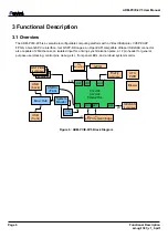
Page 9: ...requiring maintenance The ADM PCIE 9V5 also includes a fan speed controller allowing variable fan speed based on die temperature and detection of a failed fan see section Fan Controllers Figure 4 ADM...

Page 10: ...ng synchronization pulse a 12 pin header for general purpose use clocking control pins debug etc front panel LEDs and a robust system monitor XCVU5P XCVU9P FLGA2104 0 4 5 7 x8 PCIe Gen3 Edge System Mo...

Page 11: ...r Off Board will power up Immediately power down SW1 5 OFF Service Mode System Monitor normal operation System Monitor Service Mode firmware update etc SW1 6 ON HOST_I2C_EN System Monitor connected to...

Page 12: ...USER_LED_G0_1V8 User defined 0 User defined 1 D2 USER_LED_G1_1V8 User defined 0 User defined 1 D8 USER_LED_G2_1V8 User defined 0 User defined 1 D13 USER_LED_G3_1V8 User defined 0 User defined 1 D6 USE...

Page 13: ...es in the section below can be found in Complete Pinout Table FABRIC_CLK 300MHz Default IO Bank 66 25MHz 30ppm Source Si5338 Clock Synth PCIE_REFCLK MGTREFCLK0_227 MGT_PROGCLK_1 156 25 Default MGTREFC...

Page 14: ...SMON Configuration PCIE4 X1Y2 Configuration ILKN X1Y2 ILKN X1Y1 SYSMON Configuration PCIE4 X1Y0 Tandem Configuration GTY Quad 233 X1Y36 X1Y39 G RN GTY Quad 232 X1Y32 X1Y35 F RN GTY Quad 231 X1Y28 X1Y3...

Page 15: ...20 X1Y23 A RS GTY Quad 223 X1Y16 X1Y19 GTY Quad 222 X1Y12 X1Y15 GTY Quad 221 X1Y8 X1Y11 RCAL GTY Quad 220 X1Y4 X1Y7 GTY Quad 219 X1Y0 X1Y3 QSFP DD 2 lanes 4 7 QSFP DD 2 lanes 0 3 QSFP DD 3 lanes 4 7 Q...

Page 16: ...Programming Clock EMCCLK A 100MHz clock net name EMCCLK_B is fed into the EMCCLK pin to drive the SPI flash device during configuration of the FPGA Note that this is not a global clock capable IO pin...

Page 17: ...wer is valid 100ms after power is valid 20ms after PERST is released The ADM PCIE 9V5 does meet this requirement when configured from a tandem bitstream with the proper SPI constraints detailed in the...

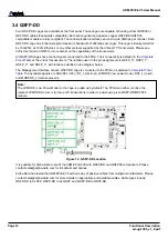
Page 18: ...s is QSFP_0 QSFP_1 QSFP_2 and QSFP_3 with locations clarified in the diagram below The Management Interface of each QSFP DD cage is connected to the FPGA as detailed in Complete Pinout Table The avail...

Page 19: ...mpliant interfaces running at 200G 8 channels at 25G Please contact support alpha data com or your IBM representative for more details on OpenCAPI and its benefits The SlimSAS connector can also be us...

Page 20: ...pin ATX Cable in amps 12V_EDGE ADC02 12V board input supply from PCIe Edge 12V_EDGE_I ADC03 12V board input current from PCIe Edge in amps 3V3_EDGE ADC04 3 3V board input supply from PCIe edge unused...

Page 21: ...irmware Flashing Red FPGA configuration cleared to protect board Table 6 Status LED Definitions 3 6 2 Fan Controllers The onboard USB bus controlled by the system monitor has access to a MAX6620 fan c...

Page 22: ...rom Flash Memory The FPGA can be automatically configured at power on from two 1 Gbit QSPI flash memory device configured as an x8 SPI device Micron part numbers MT25QU01GBBB8E12 0 These flash devices...

Page 23: ..._design set_property CFGBVS GND current_design set_property CONFIG_VOLTAGE 1 8 current_design set_property BITSTREAM CONFIG OVERTEMPSHUTDOWN Enable current_design Generate an MCS file with these prope...

Page 24: ...table for a global clock connection The direct connect GPIO signals are limited to 1 8V by a quickswitch 74CBTLVD3245PW in order to protect the FPGA from overvoltage on IO pins This quickswitch allows...

Page 25: ...ta com for front panel connector options For pin locations see signal name ISO_CLK in Complete Pinout Table The signal is isolated through a optical isolator part number TLP2367 with 220 ohm of series...

Page 26: ...HU4IGT4A The address pins A2 A1 and A0 are all strapped to a logical 0 Write protect WP Serial Clock SCL and Serial Data SDA pin assignments can be found in Complete Pinout Table with the names SPARE_...

Page 27: ...OS18 BF24 CAPI_I2C_SDA_1V8 IO_L1N_T0L_N1_DBC_64 1 8 LVCMOS18 BC23 CAPI_INT RESET_1V8 IO_L2P_T0L_N2_64 1 8 LVCMOS18 BB1 CAPI_RX0_N MGTYRXN0_224 MGT BB2 CAPI_RX0_P MGTYRXP0_224 MGT AY1 CAPI_RX1_N MGTYRX...

Page 28: ...LK_PIN_P IO_L13P_T2L_N0_GC_QBC_66 1 8 LVDS with DIFF_TERM_ADV G22 FIREFLY_INT_1V8_L IO_L13P_T2L_N0_GC_QBC_72 1 8 LVCMOS18 R21 FIREFLY_MODPRS_L IO_L3P_T0L_N4_AD15P_72 1 8 LVCMOS18 G21 FIREFLY_RST_1V8_L...

Page 29: ...IO_L15N_T2L_N5_AD11N_64 1 8 LVCMOS18or LVDS AU21 GPIO_1_1V8_P IO_L15P_T2L_N4_AD11P_64 1 8 LVCMOS18or LVDS AV24 GPIO_2_1V8_N IO_L16N_T2U_N7_QBC_AD3N_64 1 8 LVCMOS18or LVDS AU24 GPIO_2_1V8_P IO_L16P_T2...

Page 30: ...N3_227 MGT Y7 PCIE_TX0_PIN_P MGTYTXP3_227 MGT AB6 PCIE_TX1_PIN_N MGTYTXN2_227 MGT AB7 PCIE_TX1_PIN_P MGTYTXP2_227 MGT AD6 PCIE_TX2_PIN_N MGTYTXN1_227 MGT AD7 PCIE_TX2_PIN_P MGTYTXP1_227 MGT AF6 PCIE_T...

Page 31: ...P1_233 MGT F1 QSFP_0_RX6_N MGTYRXN2_233 MGT F2 QSFP_0_RX6_P MGTYRXP2_233 MGT D1 QSFP_0_RX7_N MGTYRXN3_233 MGT D2 QSFP_0_RX7_P MGTYRXP3_233 MGT N22 QSFP_0_SCL_1V8 IO_L4P_T0U_N6_DBC_AD7P_72 1 8 LVCMOS18...

Page 32: ...1 QSFP_1_RX4_N MGTYRXN0_232 MGT T2 QSFP_1_RX4_P MGTYRXP0_232 MGT R3 QSFP_1_RX5_N MGTYRXN1_232 MGT R4 QSFP_1_RX5_P MGTYRXP1_232 MGT P1 QSFP_1_RX6_N MGTYRXN2_232 MGT P2 QSFP_1_RX6_P MGTYRXP2_232 MGT M1...

Page 33: ...TYRXP2_126 MGT N46 QSFP_2_RX3_N MGTYRXN3_126 MGT N45 QSFP_2_RX3_P MGTYRXP3_126 MGT L46 QSFP_2_RX4_N MGTYRXN0_127 MGT L45 QSFP_2_RX4_P MGTYRXP0_127 MGT J46 QSFP_2_RX5_N MGTYRXN1_127 MGT J45 QSFP_2_RX5_...

Page 34: ...N MGTYRXN1_122 MGT AF43 QSFP_3_RX1_P MGTYRXP1_122 MGT AE46 QSFP_3_RX2_N MGTYRXN2_122 MGT AE45 QSFP_3_RX2_P MGTYRXP2_122 MGT AD44 QSFP_3_RX3_N MGTYRXN3_122 MGT AD43 QSFP_3_RX3_P MGTYRXP3_122 MGT AC46 Q...

Page 35: ...5328_0_REFCLK_IN_P IO_L11P_T1U_N8_GC_64 1 8 LVDS AL24 SI5328_0_RST_1V8_L IO_L24P_T3U_N10_64 1 8 LVCMOS18 T39 SI5328_1_OUT_0_PIN_N MGTREFCLK1N_126 MGT REFCLK T38 SI5328_1_OUT_0_PIN_P MGTREFCLK1P_126 MG...

Page 36: ...D_G3_1V8 IO_L17N_T2U_N9_AD10N_66 1 8 LVCMOS18 AW8 USER_LED_G4_1V8 IO_L18P_T2U_N10_AD2P_66 1 8 LVCMOS18 AW7 USER_LED_G5_1V8 IO_L18N_T2U_N11_AD2N_66 1 8 LVCMOS18 BA15 USR_SW_0 IO_L22N_T3U_N7_DBC_AD0N_66...

Page 37: ...ADM PCIE 9V5 User Manual Revision History Date Revision Changed By Nature of Change 29 Aug 2019 1 0 K Roth Initial Release Page 33 Revision Table ad ug 1385_v1_0 pdf...

Page 38: ...dinburgh EH11 1DQ UK Telephone 44 131 558 2600 Fax 44 131 558 2700 email sales alpha data com website http www alpha data com Address 611 Corporate Circle Suite H Golden CO 80401 Telephone 303 954 876...

Reviews: