ADM-PCIE-9V5 User Manual
3.2 Clocking
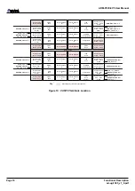
The ADM-PCIE-9V5 provides flexible reference clock solutions for the many multi-gigabit transceiver quads and
FPGA fabric. Any programmable clock, from the SI5338 Clock Synthesizer, is re-configurable from the front panel
by using Alpha Data’s avr2util utility. This allows the user to configure almost any arbitrary clock
frequency during application run time. The maximum clock frequency is 312.5MHz. Customers who purchase
RD-9V5 also have the option of embedding IP into their FPGA design that permits programmable clock
re-configuration via PCIe or from within the FPGA.
There is also two available Si5328 jitter attenuator. These can provide clean and synchronous clocks to the
QSFP-DD and OpenCAPI (SlimSAS) quad locations at many clock frequencies. These devices only use volatile
memory, so the FPGA design will need to re-configure the register map after any power cycle event.
All clock names in the section below can be found in
FABRIC_CLK 300MHz Default (IO Bank 66)
25MHz
30ppm
Source
Si5338
Clock
Synth
PCIE_REFCLK (MGTREFCLK0_227)
MGT_PROGCLK_1 156.25 Default (MGTREFCLK0_232)
0
1
2
3
PCIE_LCL_REFCLK (MGTREFCLK1_225)
PCIe
Edge
J10
(OpenCAPI)
U36
(ASFLMPLV-
100.000MHZ-LR-T)
CAPI_CLK_1 156.25MHz std. MGTREFCLK0_224)
Buffer
NB6N11S
CAPI_CLK_2 156.25MHz std. MGTREFCLK0_225)
Buffer
NB6N11S
Buffer
NB6N11S
MGT_PROGCLK_0 156.25 Default (MGTREFCLK0_121)
MGT_PROGCLK_2 156.25 Default (MGTREFCLK0_126)
Si5328_0
(2.5V VCC)
Address: 1101000
CS_CA = CMODE = GND
Other control pins = N/C
I2C
CLKOUT2
CLKOUT1
Crystal
114.285MHz
XA/XB
CLKIN1
CLKIN2
FPGA Bank 64 (LVDS)
SI5328_0_REFCLK_IN_P
SI5328_0_REFCLK_IN_N
Si5328_1
(2.5V VCC)
Address: 1101001
CS_CA = CMODE = GND
Other control pins = N/C
I2C
CLKOUT2
CLKOUT1
Crystal
114.285MHz
XA/XB
CLKIN1
CLKIN2
FPGA Bank 64 (LVDS)
SI5328_1_REFCLK_IN_P
SI5328_1_REFCLK_IN_N
FPGA Bank 64 (LVCMO18)
SI5328_1V8_SDA
SI5328_1V8_SCL
SI5328_0_OUT_0 (MGTREFCLK1_121)
SI5328_0_OUT_1 (MGTREFCLK1_232)
SI5328_1_OUT_0 (MGTREFCLK1_126)
SI5328_1_OUT_1 (MGTREFCLK1_224)
Figure 9 : Clock Topology
Page 9
Functional Description
ad-ug-1385_v1_0.pdf


