


Pinout Information
Pin Descriptions
Table 2-7
provides detailed Miscellaneous pin descriptions.
Table 2-8
provides detailed Microprocessor Debug Port pin descriptions.
PORTC0
39
I/O D5
General purpose I/O port controlled by PCDAT(7:0) and PCEN(7:0).
PORTC(7:0) can also function as:
PORTC1
40
I/O D5
PORTC2
41
I/O D5
PORTC3
42
I/O D5
PORTC4
43
I/O D5
PORTC5
44
I/O D5
PORTC6
45
I/O D5
PORTC7
46
I/O D5
RXD
67
I/O U5
Serial Receive Data. RXD is the serial receive data for the on-chip serial
port. This pin can also function as the 2-wire master data pin when
2WMEN=16.
TXD
68
I/O U5
Serial Transmit Data. TXD is the serial transmit data for the on-chip serial
port. This pin can also function as the 2-wire master clock output pin when
2WMEN=16.
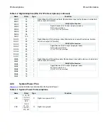
Table 2-7 Miscellaneous Pin Descriptions
Name
Pin(s)
Type
Function
TESTEN
142
ID 5
Test Mode Enable. Connect to ground for normal operation.
RESET_N
139
BOD
Bidirectional reset pin. This pin requires a pull-up resistor to V33 (VDDQ3).
The typical value is 3.3K ohm.
• When EXTRSTEN=1, RESET_N is an input.
• When EXTRSTEN=0, RESET_N is an output. In either case a low
indicates reset.
EXTRSTEN
28
ID 5
External Reset Enable.
• When EXTRSTEN=1, the internal reset is disabled and an external reset
must be supplied on the RESET_N pin.
• When EXTRSTEN=0, the internal reset is enabled and RESET_N
becomes a bidirectional pin that can be used to either drive external logic
in the system or receive an external reset signal.
XI
169
I
Crystal Input. Connect to external crystal. XI can also function as the
MCLK input LVTTL-level signal from an external oscillator.
XO
170
O
Crystal Output. Connect to external crystal.
Table 2-8 Microprocessor Debug Port Pin Descriptions
Name
Pin(s)
Type
Function
TRST_N
147
ID 5
Debug port reset (low true). Leave floating if debug port is not being used.
TCK
146
ID 5
Debug port serial data clock. Leave floating if debug port is not being
used.
TMS
145
ID 5
Debug port mode select. Leave floating or pull to ground to disable.
TDI
144
ID 5
Debug port serial data in. Leave floating if debug port is not being used.
TDO
143
I/O D5
Debug port serial data out. Leave floating if debug port is not being used.
Table 2-6 Peripheral Interface Pin Descriptions (continued)
Name
Pin(s)
Type
Function
Function
When
GBO(7:0)
48-bit graphics input mode
VB(7:0)
24-bit RGB video input mode
U(7:0)
24-bit YUV video input mode
UV(7:0)
16-bit YUV video input mode
Summary of Contents for LCT2662
Page 25: ......
Page 26: ......
Page 27: ......
Page 28: ......
Page 29: ......
Page 30: ......
Page 31: ......
Page 32: ......
Page 33: ......
Page 34: ......
Page 94: ......
Page 95: ......
Page 96: ......
Page 97: ......
Page 98: ......
Page 99: ......
Page 100: ......
Page 101: ......
Page 102: ......
Page 103: ...Input configuration Power amplifier ...
Page 104: ......
Page 105: ......
Page 106: ......
Page 107: ......
Page 108: ......
Page 109: ......
Page 110: ......
Page 111: ...Exploded View Diagram Exploded View Diagram ...


