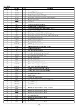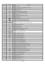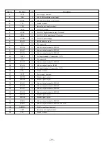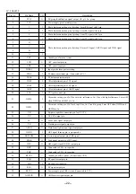
21
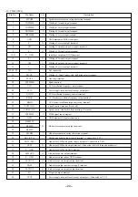
Pin No.
Pin Name
I/O
Description
87
VCC2
Power supply terminal.
88
XIN
I
16.934 MHz oscillator circuit input.
89
XOUT
O
16.934 MHz oscillator circuit output.
90
VSS
Ground terminal.
91
VDD
Internal power supply terminal.
92
AVSS
O
1 bit DAC ground.
93
OUTR
O
1 bit DAC Right channel output. (Not used)
94
OUTL
O
1 bit DAC left channel output. (Not used)
95
AVDD
O
1 bit DAC power supply.
96
MAD9
O
DRAM address output.
97
NC
I/O
Not connected.
98
MAD8
O
Address output terminal to DRAM.
99
MAD7
O
Address output terminal to DRAM.
100
MAD6
O
Address output terminal to DRAM.
101
TEST1
I
Test input terminal. (Connected to VCC)
102
NC
I/O
Not connected.
103
MAD5
O
Address output terminal to DRAM.
104
MAD4
O
Address output signal to DRAM.
105
TEST3
I
Test input terminal. (Connected to VCC)
106
VSS
Ground terminal.
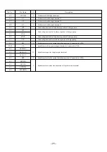
107
VCC2
Power supply terminal.
108
SMON3
O
Monitor signal output.
109
SMON2
O
Monitor signal output.
110
MAD3
O
Address output terminal to DRAM.
111
MAD2
O
Address output terminal to DRAM.
112
MAD1
O
Address output terminal to DRAM.
113
MAD0
O
Address output terminal to DRAM.
114
SMON1
O
Monitor signal output.
115
SMON0
O
Monitor signal output.
116
MAD10
O
Address output terminal to DRAM.
117
MAD11
O
Address output terminal to DRAM. (Not used)
118
ADIPWO
I
Wobble signal input terminal.
119
VDD
Internal power supply terminal.
120
VSS
Ground terminal.

