17
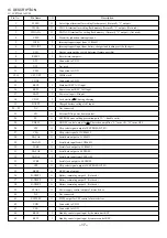
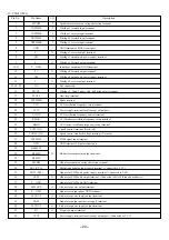
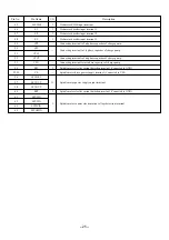
IC DESCRIPTION
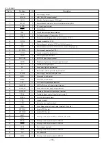
IC, LC875164A-5V90
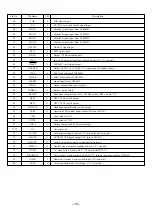
Pin No.
Pin Name
I/O
Description
1
WSEL
O
Select signal terminal for writing flash memory (Normally L output).
2
WCLK
O
CLOCK terminal for writing flash memory (Normally L output). (Not used)
3
WDATA
O
DATA I/O terminal for writing flash memory (Normally L output). (Not used)
4
EMP
I
Electricity reduction interrupt input.
5
INTB
I
Interrupt request input from LC896431.
6
CHG-INT
I
Interrupt request input from battery charge stand loading cast (both edges).
7
ECO
I
Energy saving mode switch (interrupt feature possible).
8
RESET
I
Reset micro computer.
9
XT1
Connected to VDD.
10
XT2
Not used.
11
VSS1
Connected to GND.
12, 13
CF1, CF2
3MHz clock.
14
VDD1
Connected to VDD.
15
KEY0
I
Main unit KEY A/D input.
16
KEY1
I
Remote control KEY A/D input.
17
BATT
I
Power voltage A/D input.
18
VDET
I
For detecting V during charging.
19
BATT2
I
Charged battery voltage A/D input.
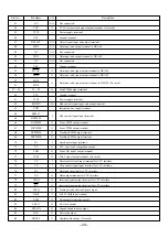
20 ~ 22
NC
Not connected.
23
PD
O
External DAC power down control.
24
PE
O
EEPROM error writing prevention port (L= disable write).
25
VDSW
O
ON/OFF control output for
V detection amplifier. L turns ON. H turns OFF.
26
CE3
O
Chip select signal output of EEPROM (IC303).
27
CEQ
O
Chip select signal of LC896431.
28
DATA0
O
Serial data output to LC896431.
29
DATAD
I
Serial data input from LC896431.
30
SCK0
O
Serial clock output to LC896431.
31
DATA2
O
Serial data output to EEPROM.
32
DATAE
I
Serial data input from EEPROM.
33
SCK2
O
Serial clock output to EEPROM.
34
CE2
O
Chip select signal output of EEPROM (IC301).
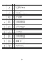
35
BEEP
O
BEEP signal output.
36
B-DISP1
O
Battery remaining output 1. (Not used)
37
B-DISP2
O
Battery remaining output 2. (Not used)
38
B-DISP3
O
Battery remaining output 3. (Not used)
39
STALL
O
Power supply control output of motor driver.
40
NC
Not connected.
41
SLPWM
O
PWM output for VM control of motor driver.
42
VDD
Connected to VDD.
43
VSS
Connected to GND.
44
KEY0
I
Standby cancel signal input by the main unit KEY.
45
KEY1
I
Standby cancel signal input by remote control KEY.

